The versatile 555 Timer IC can be used in a variety of circuits like Time Delays, Oscillation, Pulse Generation, Pulse Width Modulation etc. In this tutorial, we will learn about the Astable Multivibrator Mode of 555 Timer IC. We will learn the circuit of Astable Multivibrator using 555 Timer IC, its operation, calculate the duty cycle and also take a look at few important applications of Astable Mode of 555 Timer IC.
Astable Multivibrator Using 555 Timer IC
Astable multivibrator is also called as Free Running Multivibrator. It has no stable states and continuously switches between the two states without application of any external trigger. The IC 555 can be made to work as an astable multivibrator with the addition of three external components: two resistors (R1 and R2) and a capacitor (C). The schematic of the IC 555 as an astable multivibrator along with the three external components is shown below.
IC 555 Astable Multivibrator Circuit diagram:
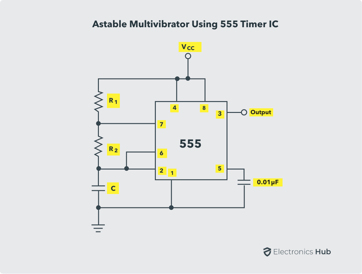
The pins 2 and 6 are connected and hence there is no need for an external trigger pulse. It will self trigger and act as a free running multivibrator (oscillator). The rest of the connections are as follows: pin 8 is connected to supply voltage (VCC). Pin 3 is the output terminal and hence the output is available at this pin. Pin 4 is the external reset pin. A momentary low on this pin will reset the timer. Hence, when not in use, pin 4 is usually tied to VCC.
The control voltage applied at pin 5 will change the threshold voltage level. But for normal use, pin 5 is connected to ground via a capacitor (usually 0.01µF), so the external noise from the terminal is filtered out. Pin 1 is ground terminal. The timing circuit that determines the width of the output pulse is made up of R1, R2 and C.
Astable Multivibrator Using IC 555 Operation
The following schematic depicts the internal circuit of the IC 555 operating in astable mode. The RC timing circuit incorporates R1, R2 and C.
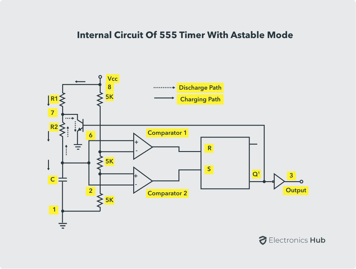
Initially, on power-up, the flip-flop is RESET (and hence the output of the timer is low). As a result, the discharge transistor is driven to saturation (as it is connected to Q’). The capacitor C of the timing circuit is connected at Pin 7 of the IC 555 and will discharge through the transistor. The output of the timer at this point is low. The voltage across the capacitor is nothing but the trigger voltage. So, while discharging, if the capacitor voltage becomes less than 1/3 VCC, which is the reference voltage to trigger comparator (comparator 2), the output of the comparator 2 will become high. This will SET the flip-flop and hence the output of the timer at pin 3 goes to HIGH.
This high output will turn OFF the transistor. As a result, the capacitor C starts charging through the resistors R1 and R2. Now, the capacitor voltage is same as the threshold voltage (as pin 6 is connected to the capacitor resistor junction). While charging, the capacitor voltage increases exponentially towards VCC and the moment it crosses 2/3 VCC, which is the reference voltage to threshold comparator (comparator 1), its output becomes high.
As a result, the flip-flop is RESET. The output of the timer falls to LOW. This low output will once again turn on the transistor which provides a discharge path to the capacitor. Hence the capacitor C will discharge through the resistor R2. And hence the cycle continues.
Thus, when the capacitor is charging, the voltage across the capacitor rises exponentially and the output voltage at pin 3 is high. Similarly, when the capacitor is discharging, the voltage across the capacitor falls exponentially and the output voltage at pin 3 is low. The shape of the output waveform is a train of rectangular pulses. The waveforms of capacitor voltage and the output in the astable mode are shown below.
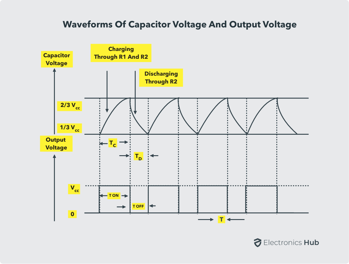
While charging, the capacitor charges through the resistors R1 and R2. Therefore the charging time constant is (R1 + R2) C as the total resistance in the charging path is R1 + R2. While discharging, the capacitor discharges through the resistor R2 only. Hence, the discharge time constant is R2C.
Duty Cycle Of Astable Multivibrator
The charging and discharging time constants depends on the values of the resistors R1 and R2. Generally, the charging time constant is more than the discharging time constant. Hence the HIGH output remains longer than the LOW output and therefore the output waveform is not symmetric. Duty cycle is the mathematical parameter that forms a relation between the high output and the low output. Duty Cycle is defined as the ratio of time of HIGH output i.e., the ON time to the total time of a cycle.
If TON is the time for high output and T is the time period of one cycle, then the duty cycle D is given by:
D = TON/ T
Therefore, percentage Duty Cycle is given by:
%D = (TON / T) * 100
T is sum of TON (charge time) and TOFF (discharge time).
The value of TON or the charge time (for high output) TC is given by:
TON = TC = 0.693 * (R1 + R2) C
The value of TOFF or the discharge time (for low output) TD is given by
TOFF = TD = 0.693 * R2C
Therefore, the time period for one cycle T is given by
T = TON + TOFF = TC + TD
T = 0.693 * (R1 + R2) C + 0.693 * R2C
T = 0.693 * (R1 + 2R2) C
Therefore, %D = (TON/ T) * 100
%D = (0.693 * (R1 + R2) C)/(0.693 * (R1 + 2R2) C) * 100
%D = ((R1 + R2)/(R1 + 2R2)) * 100
If T = 0.693 * (R1 + 2R2) C, then the frequency f is given by
f = 1 / T = 1 / 0.693 * (R1 + 2R2) C
f = 1.44/( (R1 + 2R2) C) Hz
Selection of R1, R2 and C1
The Selection of values of R1, R2 and C1 for different frequency range are as follow:
R1 and R2 should be in the range 1KΩ to 1MΩ. It is best to Choose C1 first (because capacitors are available in just a few values and are usually not adjustable, unlike resistors) as per the frequency range from the following table.
Choose R2 to give the frequency (f) you require.
R2 = 0.7 /(f × C1)
Choose R1 to be about a tenth of R2 (1KΩ min.)
R1 = 1KΩ |
R1 = 10KΩ |
R1 = 100KΩ |
|
|---|---|---|---|
(41 per min.) |
(4 per min.) |
Applications of Astable Multivibrator
Square Wave Generation
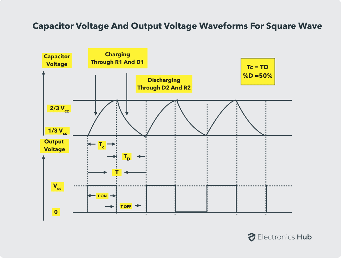
The duty cycle of an astable multivibrator is always greater than 50%. A square wave is obtained as the output of an astable multivibrator when the duty cycle is 50% exactly. Duty cycle of 50% or anything less than that is not possible with the IC 555 as an astable multivibrator mentioned above. Some modifications are to be made to the circuit.
The modification is to add two diodes. One diode in parallel to the resistor R2 with cathode connected to the capacitor and another diode in series with the resistor R2 with anode connected to the capacitor. By adjusting the values of the resistors R1 and R2, a duty cycle in the range of 5% to 95% can be obtained including the square wave output. The circuit for square wave generation is shown below.
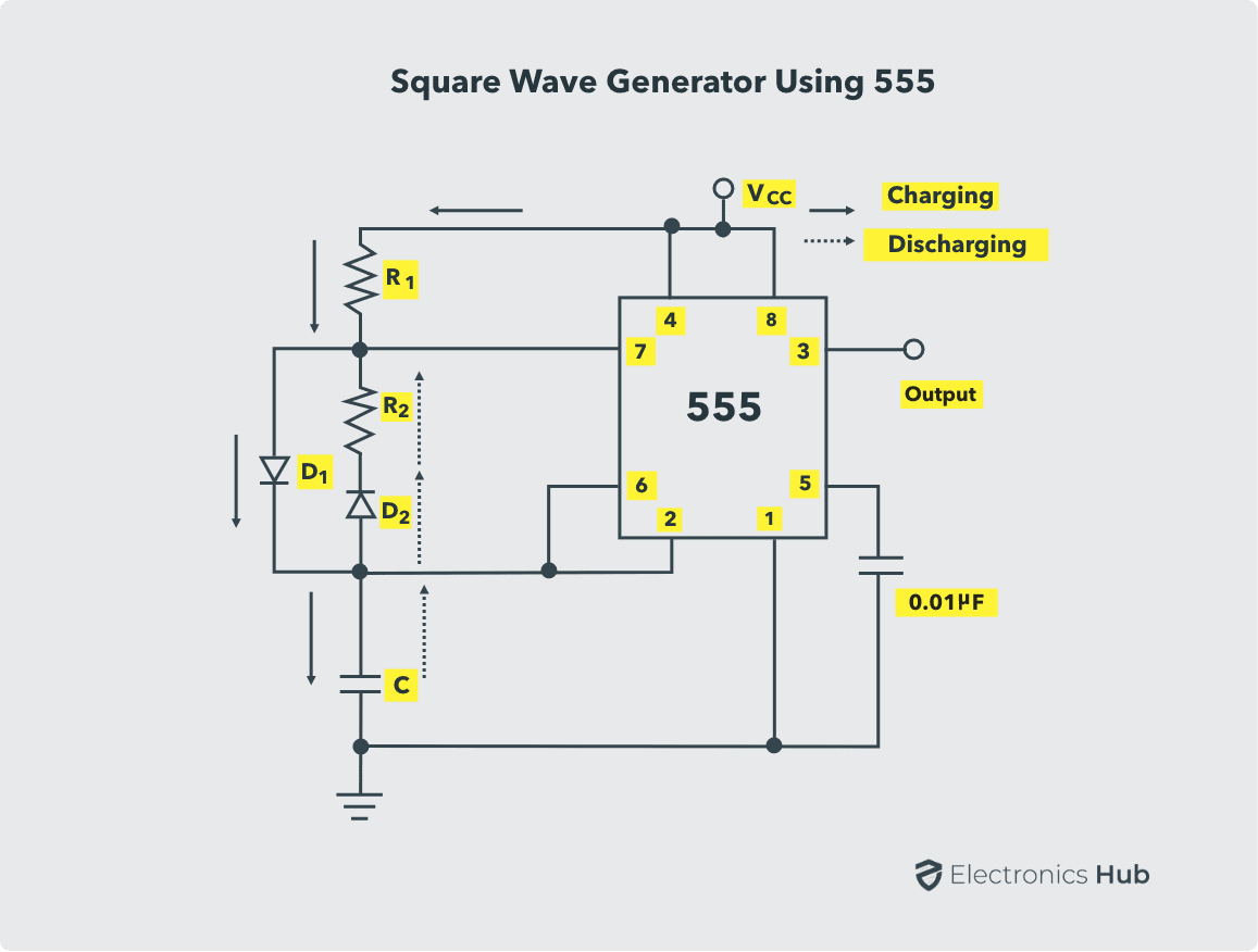
In this circuit, while charging, the capacitor charges through R1 and D1 by passing R2. While discharging, it discharges through D2 and R2.
Therefore, the charging time constant is TON = TC and is given by:
TON = 0.693 * R1 * C
And the discharging time constant TOFF = TD is given by:
TOFF = 0.693 * R2 * C
Therefore, the duty cycle D is given by:
D = R1/(R1 + R2)
In order to get a square wave, the duty cycle can be made 50% by making the values of R1 and R2 equal. The waveforms of the square wave generator are shown below.
A duty cycle of less than 50% is achieved when the resistance of R1 is less than that of R2. Generally, this can be achieved by using potentiometers in place of R1 and R2. Another circuit of square wave generator can be constructed from the astable multivibrator without using any diodes. By placing the resistor R2 between pins 3 and 2 i.e., output terminal and trigger terminal. The circuit is shown below:
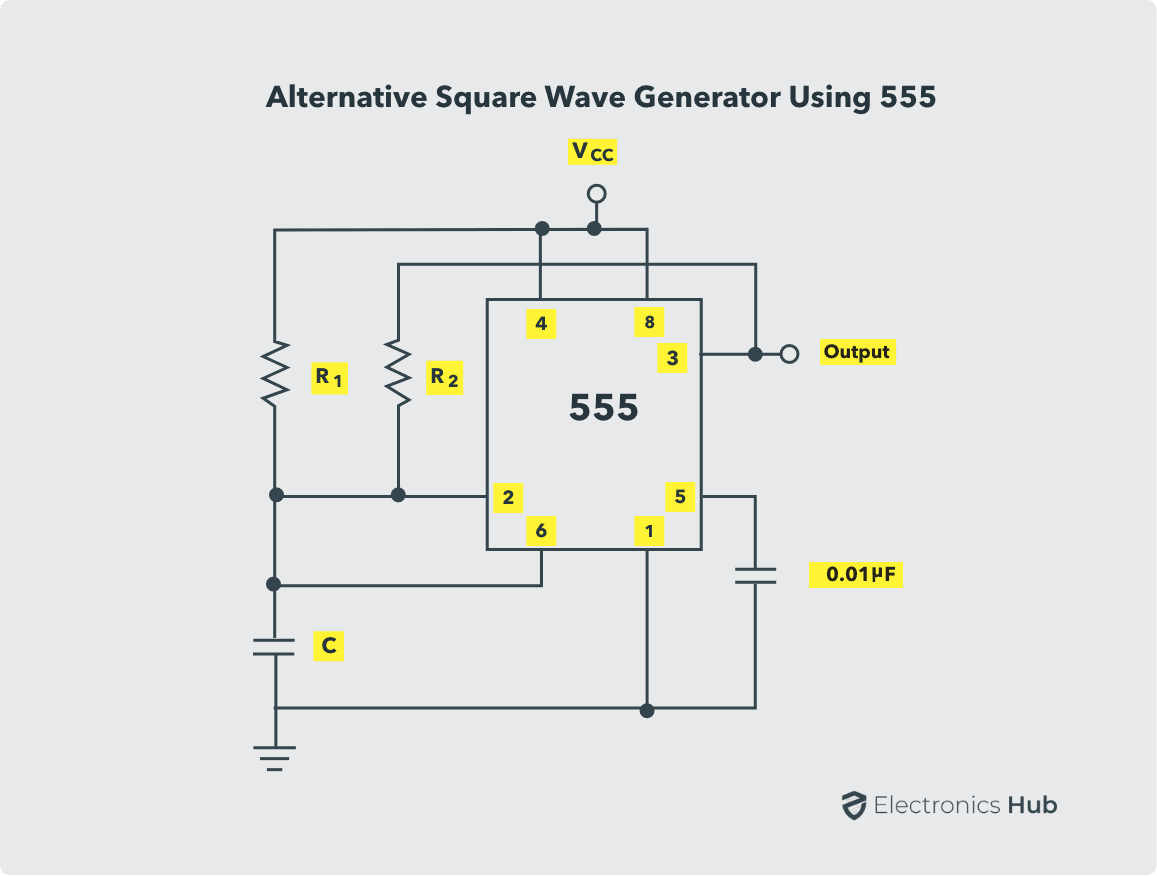
In this circuit, both the charging and discharging operations occur through the resistor R2 only. The resistor R1 should be high enough not to interfere with the capacitor while charging. It is also used to ensure that the capacitor charges to the maximum limit (VCC).
Pulse Position Modulation
In pulse position modulation, the position of the pulse varies according to the modulating signal, while the amplitude and the width of the pulse are kept constant. The position of the each pulse changes according to the instantaneous samples voltage of the modulating signal. In order to achieve Pulse Position Modulation, two 555 timer IC’s are used in which one operates in astable mode and the other in monostable mode.
The modulating signal is applied at the Pin 5 of the first IC 555 that is operating in astable mode. The output of this IC 555 is a pulse width modulated wave. This PWM signal is applied as the trigger input to the second IC 555 which is operating in monostable mode. The position of the output pulses of the second IC 555 changes according to the PWM signal, which is again dependent on the modulating signal.
The schematic of the Pulse Position Modulator using two 555 timer IC’s is shown below.
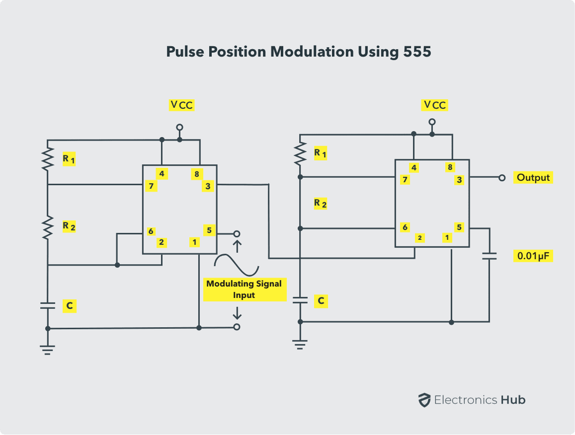
The threshold voltage for the first IC 555, which is determined by the control voltage (modulating signal), is changed to UTL (Upper Threshold Level) and is given by
UTL = 2/3 VCC + VMOD
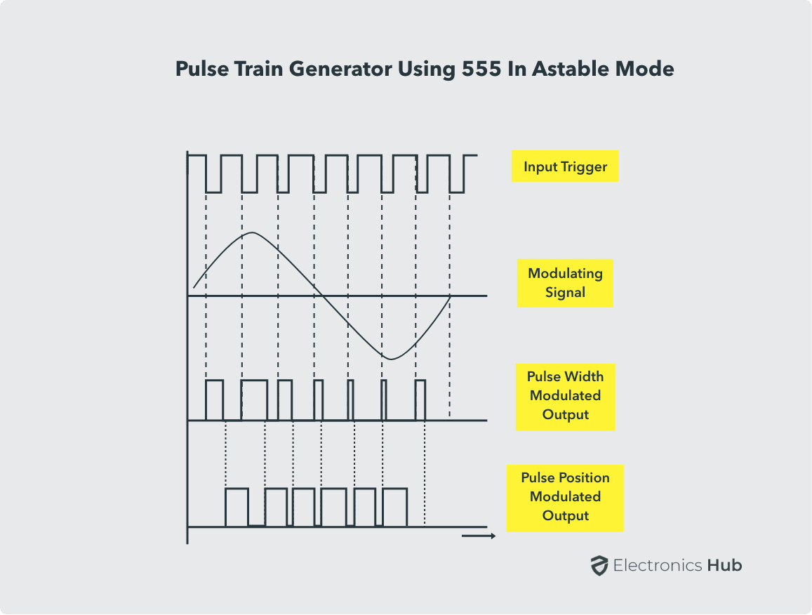
As the threshold voltage changes with respect to the applied modulating signal, the width of the pulse changes and hence, the time delay is varied. As this pulse width modulated signal is applied to the trigger of the second IC, there will be no change in either amplitude or width of the output pulse but only the position of the pulse is changed.
The waveforms of the pulse position modulated signals are shown below.
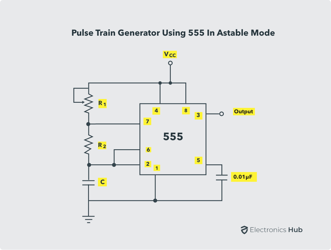
Pulse Train
We know that astable multivibrator will generate continuous stream of pulses. By using a potentiometer in place of R2, a train of pulses can be generated with different widths. The circuit pulse train generator using astable mode of operation of the IC 555 is shown below.
Frequency Modulation using Astable Multivibrator
Astable multivibrator can be used to generate frequency modulated signals. A modulating signal is given to the pin 5 (control voltage). The circuit of Frequency Modulation using astable mode of operation of the IC 555 is shown below.
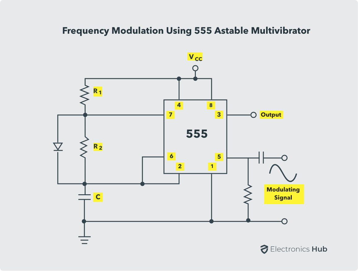
A diode is connected in parallel to the resistor R2 in order to generate a pulse output with duty cycle ≈ 50%. The modulation signal is applied at pin 5 through a high pass filter consisting of a capacitor and a resistor. According to the amplitude of the modulating signal applied at pin 5, the output will be frequency modulated.
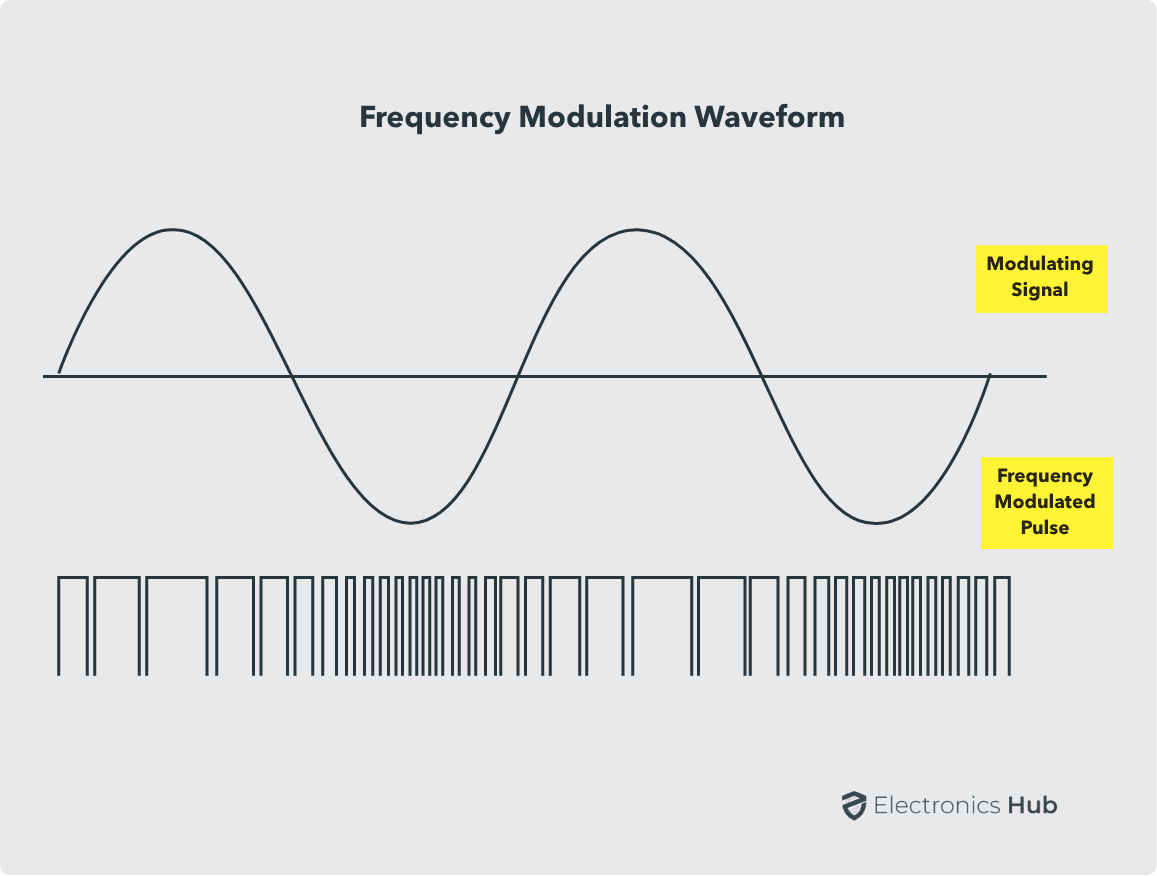
If the voltage of the modulating signal is high, the time period of the output signal is high and if the voltage of the modulating signal is low, the time period is low. The waveforms of the modulation signal and the frequency modulated signal are shown below.
Conclusion
A complete beginner’s guide on working of Astable Multivibrator using 555 Timer IC. You learned how to configure the 555 Timer to operate as an Astable Multivibrator or a Free Running Oscillator, the circuit and its operation, calculation of Duty Cycle and also some important applications of Astable Mode of 555 Timer IC.

10 Responses
good satisfactory information for a beginner.
thanks
This is the best Web…
Sir actually the capacitor blocks dc and allows a.c. whenever we are connected it in series, but according to the operation mentioned above it allows dc how Sir??
I am also a student so my answer might be completely right…
What i know is capacitor blocks dc current but according to capacitor working a potential difference is created across the plates during charging of a capacitor. This is all what is needed in ic 555 because its the potential at pins 2 and pins 6 which causes the changing in states of comparators. Their is no question of current here. And capacitor blocks dc current i.e one direction flow of electrons but not potential difference. When a capacitor charges potential difference across the plates do change without any flow of current till certain stage..
Hope this helped you
555 IC is explained in a systematic way.. Very useful information..
Very useful to me…..
Very beneficial for me!!!!!!!!!!!☺
And all the concept has explained in detail.
Thank you
Sir, in the square wave generator circuit, the capacitor may not charge to 2/3 Vcc to begin the discharge path, the drop across the diode(the led ) is not taken in account. ideally it should work, but in practical there is slight issue.
It is a helpful article
Really very very helpful.Thanks a lot.