In this tutorial, we will learn about Active Filters Design in brief. In the previous tutorial, I have discussed all the types of Active Filters i.e. High Pass, Low Pass, Band Pass and Band Stop. This tutorial will be a summary to all those individual filter concepts.
If you want more information on individual Active Filters, read these posts: “Active High Pass Filter“, “Active Low Pass Filter“, “Active Band Pass Filter” and “Band Stop Filter“.
Introduction
We have already studied the Passive RC filters such as low pass, high pass and band pass filters using resistors and capacitors. The main disadvantage of these passive filters is the output signal is less as compare to the input signal, i.e. the signal gain is never greater than unity so that load impedance affects the filter characteristics.
Output signal is attenuation is severe in multi stage passive filters. The best way to control the loss of signal is by using amplification through the use of Active Filters. Theses filter use active components such as transistors, FET’s (Field Effect Transistors), Operational amplifiers in their design. These filters draw the external power from the source to boost the output signal.
Active Low Pass Filter
Before going to know about active low pass filter, get an idea about basics of filters, passive low pass filter and frequency response.
The frequency response of Active low pass filter is same as that of the passive low pass filter, except that the amplitude of the output signals. The voltage gain of the non-inverting operational amplifier is given as
AF = 1+ (R2/R1)
The gain of active low pass filter is given as
Av = Vout / Vin = AF/ [√(1+(f/fc)²) ]
Where
- AF is the pass band gain (1+ R2/R1)
- f is the frequency of input signal
- fc is the cut-off frequency
Note:
- At very low frequencies, f < fc : Av = Vout / Vin ≅ AF
- At cut-off frequency, f = fc : Av = Vout / Vin = AF/ = 0.707 AF
- At very high frequency, f > fc: Av = Vout / Vin < AF
Active High Pass Filter
Before going to study about Active high pass filter,
The simple Active high pass filter can be obtained by connecting a non-inverting or inverting operational amplifier to the passive high pass RC circuit. The frequency response of active high pass filter is same as that of passive low pass filter, except that the magnitude of the signal is increased by the gain of operational amplifier.
In active high pass filter pass band is limited due to the open loop characteristics of operational amplifier.
The gain of active high pass filter is given as
Av = Vout / Vin = (AF (f / fc)) / (√[√(1+(f/fc)²) ]
Where
- AF is the pass band gain (1+ R2/R1)
- f is the frequency of input signal
- fc is the cut-off frequency
Voltage gain in dB is given as
Av (dB) = 20log10 (Vout/Vin)
-3dB = 20log10 (0.707 x Vout/Vin)
For a first order Active high pass filter the frequency response curve increases at a rate of 20dB/decade or 6dB/octave until it reaches the cut-off frequency point. Same as like passive filter here also cut-off frequency can be calculated using the formula
fc = 1 / (2πRC)
In this filter the phase shift or phase angle of the output signal leads that of the input signal. At cut-off frequency phase angle value is equal to the +45°. This value can be calculated using the below formula.
Phase angle Ø = tan-1 (1/ (2πRC))
We can design a single stage active high pass filter using inverting amplifier configuration also. The applications of active high pass filters also same as that of passive high pass filter.
Active Band Pass Filter
Band pass filter is frequency selective filter used in electronic systems to allow a particular band or certain range of frequencies. This range of frequencies is set between two cut-off frequency points (fL, fH).
Simple Active pass band filer can be easily designed by combining or cascading a low pass filter with a high pass filter as shown below.
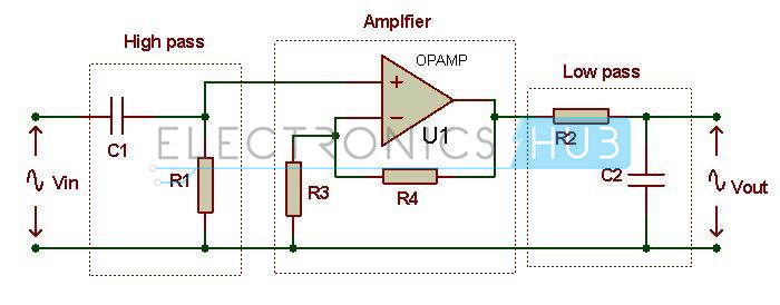
The cascade connection of low pass filter and high pass filter produces a low “Quality factor” type filter which has wide pass band. The first stage of the circuit (high pass filter stage) blocks the very low frequency signals and low pass filter stage blocks the very high frequency signals.
It produces the relatively flat pass band frequency response in which one half represents high pass filter response and other half represents the low pass filter response as shown below.
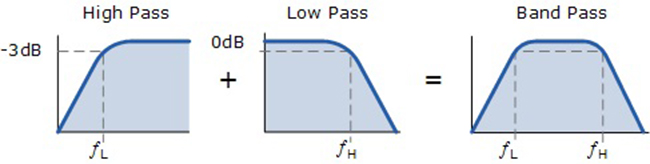
The higher cut-off frequency fH and lower cut-off frequency fL are calculated using the first order low pass and high pass filter cut-off frequency equations. The amplifier circuit provides isolation between two stages and increases overall gain of the circuit.
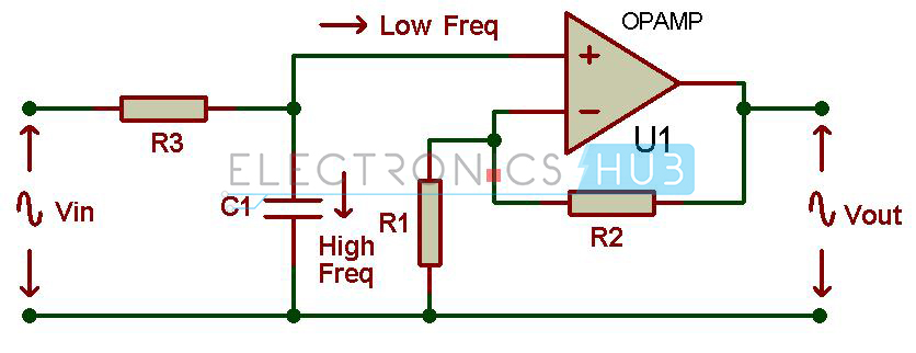
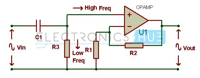
Active Band Stop or Band Reject Filter
Band stop filter attenuates only for a particular band of frequencies and allows all other frequencies. This filter is also called as band elimination filter. These are classified as
- Wide band reject filters
- Narrow band reject filters (Notch filters).
Wide band reject filter bandwidth is very high as compare to narrow band filters.
Narrow Band Filter (Notch Filter)
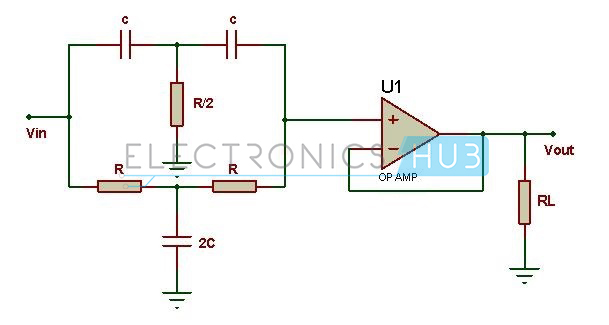
This filter is commonly used to attenuate single frequency. The main part in this circuit is Twin – T network. It consists of two T networks. First T – network is made with 2 capacitors and a resistor. Other T network is made with 2 resistors and a capacitor.
Narrow band or notch filters are commonly used in biomedical instruments and communications to remove the unwanted frequencies.
