In the early days of printed circuit board manufacturing / assembling, all the components, be it microprocessors, resistors, capacitors, connectors etc., are inserted into the holes on the board and then soldered on. But the advancement in semiconductor manufacturing led to making of smaller components and as a result, instead of inserting the components into holes on PCB, they are placed on the surface of the circuit board and soldered. This technique is simply known as SMT. But What Does SMT Mean in Electronics? Why the electronics industry moved away from through-hole components? Let us discuss all the essential things related to SMT in this article.
What Does SMT Mean in Electronics?
Before understanding SMT, let us quickly recap the other popular device mounting technology called the Through-Hole Technology. In this, the components have leads or terminals and they are inserted into the holes on the circuit board. Hence, the name “through-hole”. Once, they are inserted, the leads can be soldered to make a permanent contact.
The main problem with through-hole technology is the PCB assembling process is mainly manual with the scope of automation limited to only certain components such as integrated circuit packages. As a result, the manufacturing time and cost is high. There are some other disadvantages with through-hole technology. We will discuss them later.
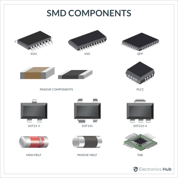
SMT is short for Surface Mount Technology. In this technique, electronics components are fixed on the surface of the printed circuit board (PCB) and their leads or terminals stay on the surface of the board to be soldered. The components that are designed to be used in Surface Mount Technology are known as Surface Mount Devices (SMD).
Surface Mount Technology is not something that has been recently developed. In fact, it has been around for more than 5 decades. Since then, SMT has seen several technical improvements in terms of components, PCB assembling or manufacturing techniques, soldering and many more.
As the system design is becoming more complex, integration of more functionality on the same PCB size is also important. If the components chosen are older through-hole style devices, then it would be difficult to place a greater number of components as through-hole components are larger in size.
This is where surface mount devices and the corresponding SMT is useful. As SMD components are very small compared to their through-hole counter parts, it is possible to place more components in a small area.
Another major benefit of SMD and SMT is automation of PCB assembly. Once the PCB is designed and manufactured, the assembly of SMD components can be automated with the help of precise pick-and-place machines. As all the components sit on the surface of the PCB, the pick-and-place machine doesn’t have to worry about any hole, but just align the components and place them properly in their designated locations.
Once all the components are placed, they are soldered using a reflow oven. The whole process of assembling can be automated including testing with minimal human intervention. This essentially, reduces errors and also significantly increases the production output. All thanks to SMT.
The Growth of SMT
In the initial years when SMT was developed, it was primarily used for military applications. But the wide development of surface mount device led Japan to invest in SMT to produce tiny and portable electronic gadgets and products.
Another major factor in shifting to SMT was the size of integrated circuits. Earlier dual-in-line package ICs were so big. But with increasing functionality of integrated circuits means the number of pins or leads are also increasing. Hence, instead of regular dual-in-line packing, semiconductor manufactures opted for surface mount packaging such as Ball Grid Array and Quad Flat Pack, which not only reduced the size of the IC but also packed more pins.
With smaller IC and components in the form of SMD devices, SMT became the dominating technology in PCB manufacturing. SMT also has the benefit of mounting components on both sides of the circuit board, which means the PCB can be made even small and compact.
Since the 80’s, the electronics industry invested heavily in SMT for developing smaller SMD devices, better soldering techniques and machines and as a whole a compact PCB.
Another major reason for the growth of SMT is the mass production of electronic products. As PCBs with through hole components involve a lot of manual work, the time spent on a PCB is significantly more. This is not feasible for mass production as it raises the overall cost of the product.
With the usage of SMD components and SMT, the process of mounting components and soldering can be fully automated. Even the job of finding faults is automated. This will reduce the manufacturing time and cost of the product.
Advantages of SMT
Here are some of the benefits of SMT over through-hole technology.
- Components are small in size as well as light in weight.
- No need to drill holes in the PCB as components mount on surface.
- Easy to assemble SMD components.
- Pick-and-place mounting process.
- Fully automated mounting and soldering.
- Easy to detect and correct component placement errors.
- PCBs can be small and compact.
- SMD components can be mounted on both sides of the PCB.
- Cost of SMD components is less than through-hole counterparts.
Disadvantages of SMT
There are some drawbacks associated with SMT as well. Here are a few disadvantages.
- Small components mean difficult for manual handling.
- Repair / rework is very difficult, especially in Ball-grid type components.
- The cost of setting up SMT assembly is very high.
Types of SMT Assembly
Depending on the design of the circuit, a PCB can contain only SMD components, SMD components on both sides of the PCB or a combination of SMD and through-hole components. Based on the type of components, there are three basic types of SMT assembly.
- Type I
- Type II
- Type III
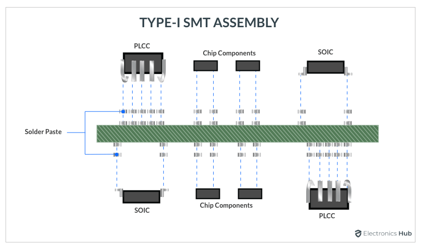
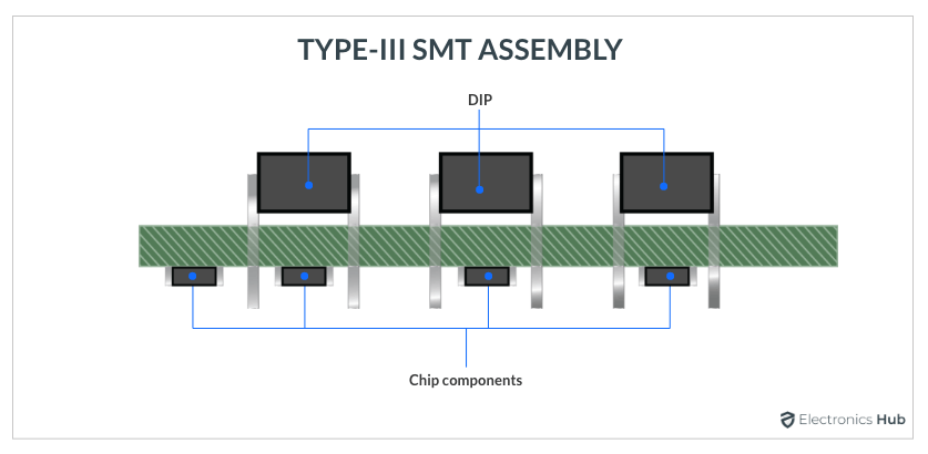
In Type I SMT Assembly, all the components are SMD and the components can be mounted on a single side or on both sides of the PCB. Coming to Type III SMT assembly, discrete SMD components such as resistors, capacitors and transistors are mounted only on the bottom side of the PCB.
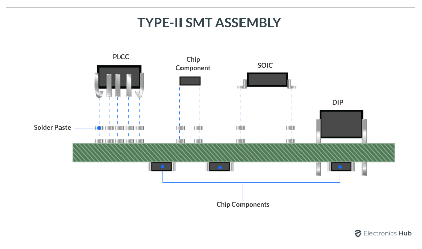
Finally, Type II is a combination of Type I and Type III. An important point about this classification of SMT assembly types is that there are no standards regarding this nomenclature.
SMT Assembling Procedure
The electronics manufacturing industry is moving towards SMT at an exponentially increasing pace. One of the main reasons for this is the significant development in the machines associated with SMT assembling. With complete machine-based assembling, the SMT has the advantage of fast manufacturing at low cost and at the same time completely automating the process.
Let us now see an abstract view of the complete SMT assembling and soldering procedure. We will also learn about different machines used in each stage of assembly. The following is the list of steps involved in SMT Assembly.
- PCB Loading
- Printing Solder Paste
- Inspecting Solder Paste
- Mounting Components
- Reflow Soldering
- Optical Inspection
- Unloading PCB
PCB Loader
Initially, after PCBs are manufactured, they are placed in the loader machine in a vertical stack. It simply takes each PCB and places it on a conveyer belt to transfer it to the next step.
There are different types of PCB loader machines and some commonly used ones are: Magazine Loader, Vacuum Loader, Gate Conveyer.
It is important to set the speed of the PCB flow as the next PCB shouldn’t arrive while the current PCB is still processing. The PCB then moves to a Screen-Printer Machine.
Screen Printing
In this machine, the solder paste is applied to the PCB using screen printing technique. A stencil is placed on top of the PCB. It has cut outs / openings at all the locations where the solder paste has to be applied. A roller will then roll on top of the PCB to apply the solder paste.
Solder Paste Inspection
This step in SMT assembling is crucial as improper application of solder paste will result in a defective PCB. Hence, once the screen printing is done, the PCB will then move to a Solder Paste Inspector machine or SPI.
In this automatic testing, the equipment looks for screen printing faults such as missing solder, uneven solder, excess solder, no solder, etc. There are two types of SPI machines: In-line SPI, which is used for 100% detection of defects and Off-line SPI, which is used for sample checking only.
Pick-and-Place Machine
The next step is mounting the components on the PCB. A Component Mounter machine or a Pick-and-Place machine is used for this purpose. Reels of different components are attached at the back of the machine. Once the PCB arrives after passing solder paste inspections, the pick-and-place robot takes the components from the reels and places them on the PCB at their designated place.
There are different types of pick-and-place machines. Some of the commonly used machines are: Gantry Type one-by-one Mount Machine, Rotary Mount Machine and Module Mount Machine. One-by-One Mount Machine, as the name suggests, places one component at a time. This is the slowest of the three and is typically used to place small number of large sized components such as LCD, Wi-Fi Modules, etc.
For less complex assembling in small to medium scale PCB Manufacturing, the Rotary Mount machine is used. A rotating drum places the components while the PCB moves accordingly in the X-Y Axis. Finally, the Module Mount Machine has the capability of being the fastest and also most efficient machines of the three. Multiple reels of components are supplied to reduce the pick-and-place time.
Reflow Oven
Once all the components are properly placed on the PCB, it is now time to solder them. For this, a Reflow Oven is used, which applies heat to the PCB to melt the solder paste and firmly solder the components. Actually, instead of applying maximum heat at once, the reflow oven has multiple zones / stages of heat.
The first stage is called a pre-heat zone, where the temperature of the PCB is gradually raised and maintained at a stable pre-heat temperature. Then, the PCB enters a high-temperature zone, where the temperature quickly ramps to peak and at this stage, the “reflow” of solder occurs as it melts and spreads across the component and the solder pad. Finally, the temperature is brought down quickly to seal the bonding. All these heating stages happen as the PCB travels on the conveyer.
Depending on the method of producing the heat, there are different types of reflow ovens. Some of commonly used ones are:
- Infrared Reflow Oven
- Laser Reflow Oven
- Heat Reflow Oven
- Vapor Phase Reflow Oven
- Nitrogen Atmosphere Reflow Oven
In infrared type reflow, a Quartz is applied with a voltage and it radiates infrared energy. The heat from this infrared radiation is used in soldering. Laser type reflow uses either 0CO2 or Nd:YAG (Neodymium:Yttrium-Aluminum-Garnet) laser to produce the heat.
Heat reflow ovens are one of the simplest as they use a fan heater to raise the temperature of the air by convection. In Vapor Phase type reflow, hot chemical vapor is blown across the PCB for soldering.
To prevent oxidation of materials, the Nitrogen based reflow uses Nitrogen gas instead of Oxygen in the internal atmosphere. With the wide-spread usage of Lead-free soldering, N2 atmosphere reflow oven became popular.
Optical Inspection
Once the PCBs come from the reflow oven, they are then sent for automatic inspection of SMT soldering. A camera takes multiple pictures in the process of inspection and finds even small faults. There are two types of Automatic Optical Inspection Machines: Off-line and in-line. In-line inspection machines are very complex with a lot of settings and options and hence they are expensive.
Conclusion
Surface Mount is an electronic package technology that mounts the components on the surface of the PCB (printed circuit board) instead of inserting them into holes. Such devices are called Surface Mount Devices (SMD). The technique of mounting components on the surface of the PCB and soldering them is called Surface Mount Technology (SMT).
Since its development in the 1950’s, SMT is continually evolving with present day ultra-fine pitch SMD components and Ball Grid Arrays (BGA). So, if you are wondering What Does SMT mean in Electronics, then it stands for Surface Mount Technology.
