This circuit will open and close the curtain of your home and office just by pushing a switch. So with the help of this unique circuit, we do not need to move from one place to open and close the curtain. This circuit is used for household use, particularly for smaller doors and windows. Due to its small size and readily available components, it can be effortlessly fixed with a curtain. You can also provide power supply to the circuit with the help of adapter existing in the market.
Curtain Opener and Closer Circuit Diagram:
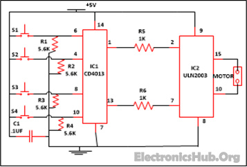
Components In Curtain Opener and Closer Circuit:
- IC
- IC1 (CD4013)
- IC2 (ULN2003)
- Resistor
- R1-R4 (5.6k)
- R6, R5 (1K)
- C1 (. 1uf)
- Stepper Motor
Description:
This circuit is made up of two ICs named CD4013 and ULN2003 with few more easily available components.
CD4013 IC contains two self-governing D type flip flop on a single chip which exists in one of two states that is 0 or 1 and can store information. Each module is further capable of group of pin outs assigned as data, set, reset, clock input and a couple complementary output Q and ![]() .
.
How D Type Flip Flop Works:
D type flip flop has one input referred to as D input or data input. The truth table of D type flip flop is shown below:
This is equivalent to saying that input data appear at the output, at the end of the clock pulse. Thus the transfer of data from input to output is delayed and hence delay (D) flip flop. That’s why it is used as a delay device or latch to store 1 bit binary information. In this clock (CK) input line controls the flip flop which is used to determine whether the input data is recognized or ignored. The input is normally a clock signal. If the clock input is binary high means logic 1 the data on the D line is stored in the flip flop. As long as clock line is high the normal output will simply follow or track the D input. If the CK line is low or it is binary 0 the D input line is recognized. Means the bit store in the flip flop previously retained. The D line can do anything. It will ignore if CK is low.
CD 4013 comes in 14 pin dual inline package. Before understanding the working of circuit diagram first have a look at its pin layout.
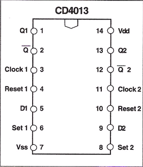
- Pins 1, 2, 13 and 12 are known as complimentary outputs hence both are presented as output but with inverse of each other. Like for first flip flop Q is 1 then
 will be 0. The same is also there for another set of flip flop.
 - Pin 5 and 9 are known as Data pins they are normally connected to one of the outputs can be Q or enlargingnction of enlargement the appsquare wavesclock for square wave and for other waves they may be ended to any other logic level means they may be either connected to supply line or to the ground of the circuit. In our circuit we have attached and Data pin 5 as one.
- Pin 3 and 11 are known as Clock input. It is used to receive the input signal for working of D type flip flop. You can provide signals with the help of transistor configured as astable multivibrator or you can provide signals through logic gate like by NANA gate or NOR gate. In our circuit we are providing the clock input with the help transistor.
- Pin 4, 6 and 10, 8 are known as set and reset pin whenever any one of the pin goes high we will receive the output. For protection these pins are assigned to a logic level normally they are grounded with a high value resistor. Once this is completed the input can be made to alternately react to positive peak pulses to control the logic stage of the Q and output alternately.
- Pin 14 and 7 are called supply and ground pin respectively. Pin 14 receives the power supply input that is Vcc which should not be more 15V otherwise it will tear down the IC and pin 7 is ground and it should be connected to the negative supply input of IC.
And ULN2003 is basically a Darlington array of high voltage as well as of high current every ULN2003 IC comprise seven unlock collector Darlington couples along with common emitter. ULN2003 is furthermore commonly used in a large variety of loads with the assist of relay drivers or may be employed to drive a stepper motor. ULN2003 works with 5V TTL and CMOS logic devices. Each channel or else Darlington couple in ULN2003 is marked at 500mA and be able to resist peak current of 600mA.Below pin diagram of IC ULN2003 is shown:

Working on this circuit is very easy to understand. Assemble the circuit properly and cross check the connection. In this circuit we are utilizing both the flip.
If you want to open the curtain just press switch S1 for some time. This will supply the voltage to pin 6 of IC1 (which is set pin) as one end of the switch is connected with power supply and when pin 6 goes high it will provide you the highest output at pin 1 of IC1 that is at Q output. Which in turn makes the pin 2 of IC2 also high and the geared motor connected at the output start revolving in the close wise direction to open the curtain. Now when the curtain is open properly or you want to stop the motor in between just press the switch S2 connected at pin 4 of IC1 which is reset pin and this is used to off or stop the stepper motor when the curtain in fully open or you want to stop in between.
A similar occurrence will happen if you want to close the curtain. Just press switch S3 for some time connected to pin 8 of IC1 which is also a set pin. Geared motor starts running in anticlockwise direction. Now when the curtain is close or you want to stop in between press the switch S4 to off the stepper motor. Therefore you can now open and close your curtain just by sitting in one place, without moving just by pressing the switch.
Are you interested to know more about Flip Flops? Then read the following posts:

12 Responses
I want to kniw that in the circuit from where we give input voltage into the circuit.
Plzz rply me
circuit me do terminal open hai.
1. +5v
2. symbol of ground.
en do terminal se 5 volt dc supply deni hai ground negative aur +5 positive
Very much useful..
Is this curtains on and off circuit is working I think so it is not. Did u get the output my friend please reply me if I the get the output means
can you show me the circuit that operates automatic..!!?
what type of stepper motor used? Does it is appropriate to use 9 V Dc motor?
Please explain how to have an output in the uln2003 pin 10 and 15 beacause i cannot have any output in it
Can a servo motor be used as an alternative?
Yes. But you need a PWM Signal to control the Servo.
whats types of switch in this circuit diagram?
what type of stepper is used ? bipolar or unipolar? tyy
Can we get a tutorial display for the circuit connections.??