In this tutorial, I will show you how to configure and use a Timer in LPC1768 Arm Cortex-M3 MCU. Timers are one of the important peripherals of modern microcontrollers. They are used to generate periodic interrupts (in ‘Timer’ mode) and also count events (in ‘Counter’ mode). Using this LPC1768 Timer Tutorial, you can generate precise delays, which are non-blocking delays (in contrast to hardcoded delay function).
IMPORTANT NOTE: I have mentioned this already in the previous tutorials but I will repeat it in every LPC1768 Tutorial. Download both the Datasheet and User Manual for LPC1768 MCU from the official NXP website. I cannot explain / discuss each and every topic in detail. You have to look up for the topic of discussion in those documents and gather additional information.
Introduction
The Timer is a crucial hardware component of microcontrollers. Usually, Timers are used to measure elapsed time like processor ticks or count external events. Hence, the name Timers and Counters interchangeably used in embedded systems. The timer peripheral is an integral part of a large number of applications ranging from simple LED Control and periodic event generation to complex motor control applications.
If you remember the LPC1768 GPIO Tutorial, I have given a simple LED Blinky program with hardcoded delay. This method of hardcoding delays is not desirable as it blocks the processor during the period of delay and doesn’t allow any other operations (like interrupts).
The correct way to generate delays is using the Timer peripheral of the MCU. Delays generated using Timers are very precise and are also non-blocking i.e. they allow interrupts.
Timer in LPC1768
There are four identical Timer peripherals in LPC1768 viz. Timer0, Timer1, Timer2 and Timer3. All four timers are 32-bit timers with programmable 32-bit prescaler.
They are designed to count cycles of the peripheral clock or an external clock signal and optionally generate interrupts (or other actions) at specified timer values (based on four match registers).
Of all the Timer registers in LPC1768, the Timer Counter (TC) and Prescale Register (PR) are particularly important as they are directly responsible for the Timer’s functionality. After a Timer peripheral is reset and enabled, its TC register is initialized to 0 and is incremented by 1 for every PR+1 clock cycles. After reaching its maximum, the value in TC is reset to 0 and the counting restarts.
PR register controls the resolution of the timer. For example, when PR is set to 0, then TC increments at every cycle of the peripheral clock. Similarly, if PR is set to 1, then TC increments at 2 cycles of the peripheral clock. Using these two registers we can generate precise delays.
Another important register associated with Timers is the Match Register. There are four match registers for each timer peripheral. Users can load the values into these match registers and for every TC increment, the value in TC is compared to the value in match register.
If the values are a match, then the match register can perform any of the following action:
- An interrupt is generated.
- The TC will be reset
- TC and PR will be stopped and corresponding TCR will be set to 0.
Additionally, when the values in Match Register and TC matches, you can also control the External Match Register (EMR) to set an External Match Output pin as LOW, HIGH or Toggle.
Timers 0, 1 and 3 have two External Match Outputs each while Timer 2 has four External Match Outputs.
Using this functionality, we can toggle an LED connected to one of the Match Output Pins without intervention from the processor or any GPIO functionality.
LPC1768 Timer Pins
The Timer in LPC1768 MCU has two sets of pins associated with it. One set of pins are Capture Input Pins while the other set of pins are External Match Output Pins. The following table shows the pin mapping of the Timer Peripheral with the port pins of LPC1768.
The naming convention for the pins names of the timer peripheral is as follows:
CAPx.y means Capture Input y of Timer x.
CAP0.0
P1.26
CAP0.1
P1.27
CAP1.0
P1.18 / P1.28 / P2.6
CAP1.1
P1.19 / P1.29
CAP2.0
P0.4
CAP2.1
P0.5
CAP3.0
P0.23
CAP3.1
P0.24
MAT0.0
P1.28 / P3.25
MAT0.1
P1.29 / P3.26
MAT1.0
P1.22
MAT1.1
P1.25
MAT2.0
P0.6 / P4.28
MAT2.1
P0.7 / P4.29
MAT2.2
P0.8
MAT2.3
P0.9
MAT3.0
P0.10
MAT3.1
P0.11
As you can see from the above table, there are many pins associated with the timer peripheral. Appropriate pins must be selected using PINSEL Registers.
Timer Registers of LPC1768
Each peripheral in the LPC1768 MCU has 15 registers each. I will now try to explain the functions of some of the important register associated with Timers in LPC1768.
TCR – Timer Control register: Used to control Timer Counter functions i.e. enable, disable and reset.
Bit 0
Counter Enable
When 1, TC and PR are enabled for counting. When 0, TC and PR are disabled.
Bit 1
Counter Reset
When 1, TC and PR are reset on next positive edge of PCLK. The counters remain reset until this bit is returned to 0.
TC – Timer Counter Register: It is a 32-bit register and is incremented at every PR+1 cycles of PCLK. Unless it is reset in the middle, it reaches its maximum 0xFFFFFFFF and wraps back to 0 and begins incrementing again.
PR – Prescale Register: It is a 32-bit register and specifies the maximum value for the Prescale Counter (PC). When PC value is equal to the value in PR, TC is incremented in the next clock cycle and also PC is cleared.
PC – Prescale Counter Register: It is a 32-bit register. The value in PC is incremented on every PCLK cycle and when its value matche the value in PR, the TC is incremented and the value in PC is rest on the next PCLK cycle. When PR is 0, TC increments on every PCLK cycle. When PR is 1, TC increments for every 2 PCLK cycles.
MCR – Match Control Register: Used to control the operation on the TC when one of the Match Register matches with TC.
Bits [2:0] are used for MR0, Bits [5:3] are used for MR1, Bits [8:6] are used for MR2 and Bits [11:9] are used for MR3. Remaining bits are reserved. Let us see the actions for one match register MR0.
Bit 0
MR0I
When 1, an interrupt is generated when MR0 matches with TC.
Bit 1
MR0R
When 1, reset TC if MR0 matches with TC.
Bit 2
MR0S
When 1, stop TC and PR and set TCR[0] to 0 if MR0 matches with TC.
Similarly, other bits are used to control operation on other Match registers.
MR0 – MR3 – Match Registers: Contains user loaded values to be compared with TC. When value in Match Register matches with TC, appropriate action can be performed as directed by MCR register.
EMR – External Match Register: Controls the External Match Pins MAT0.0, MAT0.1, MAT1,0, etc. Bit 0 controls the MATx.0 Pin of the Timerx and the value of this bit is determined by the bits [5:4].
External Match Outputs
External Match Bit in EMR
Control Bits in EMR
Value in Control Bits
Action on External Match Pins / Bits
MATx.0
0
5:4
00
Do nothing
01
Clear the Bit
10
Set the Bit
11
Toggle the Bit
Similarly,
- MATx.1, External Match Bit is 1 and Control bits are [7:6].
- MATx.2, External Match Bit is 3 and Control bits are [9:8].
- MATx.3, External Match Bit is 4 and Control bits are [11:10].
NOTE: MATx.2 and MATx.3 are available only for Timer 2.
CTCR – Count Control Register: Used to select either Timer Mode or Counter Mode. If counter mode is select, you can also select the input capture pin as well as the edge for counting (rising, falling or both).
When 00, CAPx.0 pin for Timerx. When 01, CAPx.1 pin for Timerx.
Bits [1:0]
Counter/Timer Mode
When 00, Timer Mode. When 01, Counter Mode with rising edge. When 10, Counter Mode with falling edge. When 11, Counter Mode with both edges.
Bits [3:2]
Counter Input Select
Calculating Timer Prescaler
First, we have to select the peripheral clock for the Timer. This is done with the help of PCLKSEL0 and PCLKSEL1 registers. The following table shows the PCLKSEL Register bits for each timer.
Timer0
PCLKSEL0 [3:2]
Timer1
PCLKSEL0 [5:4]
Timer2
PCLKSEL1 [13:12]
Timer3
PCLKSEL1 [15:14]
The value in these PCLKSEL bits will determine the final PCLK of the Timers.
00
PCLK = CCLK / 4 (Default)
01
PCLK = CCLK
10
PCLK = CCLK / 2
11
PCLK = CCLK / 8
After the PCLK is finalized, we can calculate the Prescaler Value.
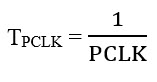
The time period of one clock cycle is given by:
The minimum time duration (or the resolution of the Timer) produced by a Timer for a given PCLK and PR values is given by:
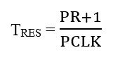
From this, we can calculate the PR value for various timer resolutions. For example, if we want 1 milli second resolution on a timer with 25 MHz PCLK, then
PR = (25 * 106 * 1 * 10-3) – 1 = 24999
Initialize TIM0 in LPC1768
First, enable TIM0 in PCONP register. On reset, both TIM0 and TIM1 are enabled.
LPC_SC->PCONP |= (1<<1);
Set the PCLK as CCLK / 4. This is set by default.
LPC_SC->PCLKSEL0 &= ~(0x3<<3);
Set Timer Mode in CTCR Register.
LPC_TIM0->CTCR = 0x0;
Set the Prescaler value in PR Register. Based on above calculations, for 1 milli second resolution, TC must increment for every PR+1 i.e. 24999+1 clock cycles.
LPC_TIM0->PR = (25000 – 1);
Finally, reset the timer to reset TC and PR values.
LPC_TIM0->TCR = 0x02;
Generate Delay using LPC1768 Timers
Let us now see how can we generate a delay in milli seconds using Timers. Let me use TIM0 as an example. Also, perform the previous initialization step before proceeding.
First, reset the timer.
LPC_TIM0->TCR = 0x02;
Then, enable the timer.
LPC_TIM0->TCR = 0x01;
In order to generate “milliseconds” amount of delay, compare the TC value to the “milliseconds” and once they match, exit and disable the timer.
while(LPC_TIM0->TC < milliseconds);
LPC_TIM0->TCR = 0x00; //Disable timer
Example
Using the above two cases, let us blink an LED using a delay generated using Timers.
#include <lpc17xx.h>
#define PRESCALE (25000-1)
void delayms(unsigned int milliseconds);
void Timer0_Init(void);
int main(void)
{
Timer0_Init();
LPC_GPIO0->FIODIR = (1<<22);
while(1)
{
LPC_GPIO0->FIOSET = (1<<22);
delayms(1000);
LPC_GPIO0->FIOCLR = (1<<22);
delayms(1000);
}
return 0;
}
void Timer0_Init(void)
{
LPC_SC->PCONP |= (1<<1);
LPC_SC->PCLKSEL0 &= ~(0x3<<3);
LPC_TIM0->CTCR = 0x0;
LPC_TIM0->PR = PRESCALE;
LPC_TIM0->TCR = 0x02;
}
void delayms(unsigned int milliseconds)
{
LPC_TIM0->TCR = 0x02;
LPC_TIM0->TCR = 0x01;
while(LPC_TIM0->TC < milliseconds);
LPC_TIM0->TCR = 0x00;
}
Conclusion
A simple tutorial on how to use a Timer in LPC1768 MCU. This LPC Timer Tutorial also explain how to generate precise delays using Timer Peripheral instead of hardcoded delay function.
