In this tutorial, we will begin exploring a completely new domain of Microcontrollers called the ARM Cortex-M3 Series. To be more specific, we will take an MCU based on ARM Cortex-M3 Architecture and explore its features, functionalities and programming. For this purpose, I have chosen the LPC1768 MCU from NXP. In this Getting Started with LPC1768 guide, I will talk about the specifications of LPC1768 MCU, its internal block diagram, memory map and list out some of its generic applications.
Why Did I Choose LPC1768?
Before I explain the reason, let me take you through some basics of ARM Cortex-M Series. It is a group of 32-bit RISC based ARM processor Cores designed and licensed by Arm Holdings. The Cortex-M Series Cores are designed for low cost and low power Microcontrollers, which can be used in a wide range of embedded applications.
Within the Cortex-M Series, there are several grades like the Cortex-M0, M3, M4, M7 etc. Each of these variations have several functional or implementational differences and are designed for a specific set of applications. For example, the ARM Cortex-M3 variants have a 3-stage instruction pipeline and doesn’t support either Floating Point Instructions or DSP Instructions. But the ARM Cortex-M7 variants have a 6-stage pipeline and supports both Floating Point as well as DSP instructions.
Let us now focus on the architecture of this tutorial series i.e. the ARM Cortex-M3. It is the first series in the entire ARM Cortex-M line-up and is primarily targeted at 32-bit Microcontroller market. The ARM Cortex-M3 based MCUs have integrated many features that are once found only in high-end microprocessors.
ARM Cortex-M3 Core is designed and developed as a successor to the famous ARM-7 Architecture. It introduced several features like non-maskable interrupts, nested vector interrupts, atomic bit manipulation and memory protection. All these and many other features make the ARM Cortex-M3 Core a very famous and widely used ARM Architecture in the Microcontroller market.
Semiconductor Manufacturers acquire license from Arm Holdings for the ARM Cortex-M3’s IP in the form of Verilog RTL (This is the Processor Core). They then modify (or optimize) the architecture as per their requirements but strictly following the Arm guidelines (This is the main Processor). Additionally, they add their own flavour of peripherals to make a complete Microcontroller Unit.
Some of the prominent vendors of ARM Cortex-M3 based MCUs are STMicroelectronics, NXP, Texas Instruments, Infineon, Microchip (Atmel), Toshiba, Analog Devices etc.
In this series of ARM Cortex-M3 Tutorials, I have chosen the LPC1768 MCU from NXP. Even though it is based on ARM Cortex-M3 Architecture, I feel that it is fairly a simple device in terms of its SFR (Special Function Registers) implementation, good support for hardware (development boards and debuggers) as well as software (IDEs and Simulators), good documentation and well written peripheral libraries.
The Right Way to Learn LPC1768 (or any ARM Device)
Learning about a new device and that too a complex device like an ARM Cortex-M3 based MCU is fairly a challenging task. First of all, the documentation is nightmarish. You first need the ARM Architecture Reference manual, then the ARM Core TRM (Technical Reference Manual), then the ARM Core Generic User Guide. This is just from the ARM side.
Then we have the vendor specific documentation like the Reference Manual, User Guide and Datasheet. But reading all these bundles of documentation isn’t going to be helpful. First of all, no one (not even the top application developers) reads the complete documentation (and I suggest you not to read the entire documentation). You will have to learn a habit of reading just the necessary part and ignoring the rest (at that particular moment).
There is also an advantage in learning a complex device like LPC1768, an ARM Cortex-M3 MCU. Due to its complexity, architecturally, all ARM Cortex-M3 devices, including the LPC1768, is neatly organized into several “functional blocks”. Each block has its own set of registers and works fairly independent to other blocks.
For example, take the LPC1768 itself. It has a Clock Generation Unit for producing the main system clock, a GPIO Unit for interfacing various peripherals, a UART Peripheral for Serial Communication and many more. If you want to learn about the GPIOs, then you can strictly focus on the GPIO Unit, its registers and how to manipulate them.
In this way, you can go through each peripheral and in the process, you can understand how these peripherals are dependent on each other, how they communicate (with each other as well as with the main processor) and how can we use them in harmony to develop our applications.
Specifications of LPC1768
NXPs LPC1768 is an ARM Cortex-M3 based Microcontroller in the LPC1700 Series. Its CPU Frequency can be as high as 100 MHz. The main processor core, which is the Arm Cortex-M3, is based on Harvard Architecture with three buses one each for instructions, data and peripherals.
Speaking of peripherals, the LPC1768 MCU consists of the following peripherals: 512 kB Flash, 64 kB RAM, USB Interface, Ethernet MAC, 4 UARTs, 2 CANs, 3 I2C Interfaces, SPI, 2 SSP Controllers, 2-input 2-output I2S, 8-channel ADC with 12-bit resolution, 10-bit DAC, 4 Timers, 8-channel DMA, 6-channel PWM, Motor Control PWM, low-power RTC, Quadrature Encoder and 70 GPIO Pins.
The following is a small list of the specifications of the LPC1768 MCU. For complete details, I suggest you to refer to the data sheet.
- ARM Cortex-M3 Processor with built-in NVIC and MPU and CPU Frequency of 100 MHz.
- On-chip Bootloader for in-system programming (ISP) and in-application programming (IAP).
- 512 kB of on-chip Flash and 64 kB of on-chip SRAM.
- 8-channel DMA Controller that can be used with ADC, DAC, Timers, UART, SSP, I2S.
- Multilayer AHB Matrix Interconnect with separate bus for AHB Master (CPU, DMA, Ethernet and USB). Split APB Bus for all other peripherals.
- Serial Interfaces
- Ethernet MAC with RMII Interface
- Full-speed USB 2.0 Controller
- Four UARTs
- 2-channel CAN Controller
- 2 SSP Controllers
- 3 I2C Interfaces
- SPI
- I2S
- Other Peripherals
- 70 GPIO Pins
- 8-channel 12-bit ADC
- 10-bit DAC
- 4-Timers
- Dedicated PWM Block
- Motor Control PWM
- Quadrature Encoder Interface
- RTC
- WDT
Block Diagram of LPC1768
The following image shows the internal block diagram of the LPC1768 MCU. As you can see from the block diagram, the ARM Cortex-M3 Processor consists of three buses: I-code bus (for Instruction Fetch), D-code bus (for Data Access) and System Bus (for peripheral access).
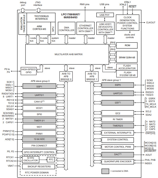
The Multi-layer AHB Matrix is used to connect the three buses of the ARM Cortex-M3 as well as the other Bus Masters (i.e. DMA, USB and Ethernet) to the rest of the peripherals.
Memory Map of LPC1768
The LPC1768 MCU, like the other ARM Cortex-M3 MCUs, incorporates several memory regions for Flash, RAM, AHB Peripherals and APB Peripherals. Since it is a 32-bit architecture, the LPC1768 has a 4 GB address space.
Following image represents the overall memory map for the entire 4 GB address space.

Applications of LPC1768
The LPC1768 MCU, being an ARM Cortex-M3 based Microcontroller, is powerful enough to run pretty complex embedded applications. Some of the common applications of this MCU are listed below:
- Motor Control
- Alarm / Security Systems
- Industrial Networking
- Lighting Control Units
- eMetering Equipment
- Consumer grade Refrigeration and Washing Units
Conclusion
This is a simple tutorial for Getting Started with LPC1768 MCU. In this tutorial, I have given a brief introduction to the ARM Cortex-M3 based LPC1768 MCU from NXP along with some important specifications. I suggest you to download the Datasheet as well as the User Manual for LPC1768 as they are the go-to guide for all the necessary information.
In the upcoming tutorials, I will take up some important peripherals of LPC1768 and try to explain how to configure them by accessing the corresponding registers.
Hardware and Software Suggestions
As a part of this Getting Started with LPC1768 guide, I would like to make some suggestions on the hardware and software used for developing LPC1768 Applications.
Since all the LPC1768 MCUs come with UART Bootloaders, any development board with LPC1768 MCU and an UART to USB interface on-board will be sufficient. You don’t need a high-end or a costly development board.
Coming to the software, I prefer to use the Keil MDK IDE for writing and debugging the C Code for LPC1768. In order to program the LPC1768 MCU, I will be using the Flash Magic programming tool, which is designed specifically for NXP Microcontrollers with UART Bootloaders.
If you are interested, you can buy a JTAG Debugger for ARM Microcontrollers. But this is optional and you can get away with the simulator feature of Keil MDK.

One Response
it was a useful tutorial sir ,produce more.