In this Transistor tutorial, we will learn about the working of a Transistor as a Switch. Switching and Amplification are the two areas of applications of Transistors and Transistor as a Switch is the basis for many digital circuits. We will learn different operating modes (Active, Saturation and Cut-off) of a Transistor, how a transistor works as a switch (both NPN and PNP) and some practical application circuits using transistor as a switch.
Transistors
Transistors is a three-layer, three-terminal semiconductor device, which is often used in signal amplification and switching operations. As one of the significant electronic devices, transistor has found use in enormous range of applications such as embedded systems, digital circuits and control systems.
You can find Transistors in both digital and analog domains as they are extensively used for different application usage like switching circuits, amplifier circuits, power supply circuits, digital logic circuits, voltage regulators, oscillator circuits and so on.
This article mainly concentrates on the switching action of the transistor and gives a brief explanation of transistor as a switch.
A Brief Note on BJT
There are two main families of Transistors: Bipolar Junction Transistors (BJT) and Field Effect Transistors (FETs). The Bipolar Junction Transistor or simply BJT is a three-layer, three terminal and two junction semiconductor device. It consists of two PN Junctions coupled back-to-back with a common middle layer.
Whenever we say the term ‘transistor’, it often refers to BJT. It is a current controlled device, where the output current is controlled by the input current. The name bipolar indicates that two types of charge carriers i.e., Electrons and Holes conduct current in the BJT, where holes are positive charge carriers and electrons are negative charge carriers.
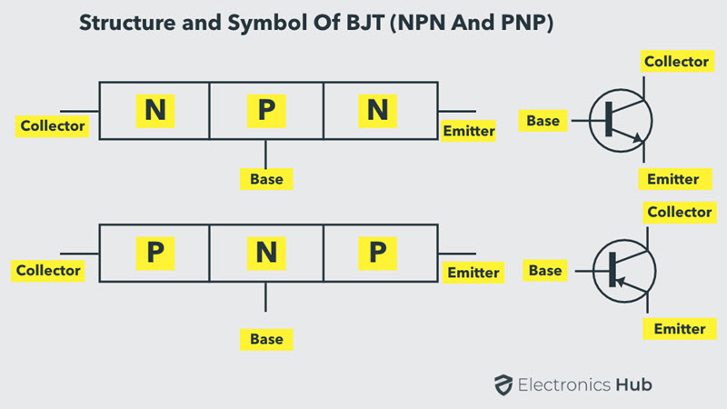
The transistor has three regions, namely base, emitter and collector. The emitter is a heavily doped terminal and emits electrons into the base. Base terminal is lightly doped and passes the emitter-injected electrons on to the collector. The collector terminal is moderately doped and collects electrons from base. This collector is large when compared to the other two regions so it can dissipate more heat.
BJTs are of two types: NPN and PNP. Both these function in the same way but they differ in terms of biasing and power supply polarity. In PNP transistor, N-type material is sandwiched between two P-type materials whereas in case of NPN transistor P-type material is sandwiched between two N-type materials.
These two transistors can be configured into different types like common emitter, common collector and common base configurations.
If you are looking for working of MOSFET as a Switch, then first learn the basics of MOSFET.
Operating Modes of Transistors
Depending on the biasing conditions like forward or reverse, transistors have three major modes of operation namely cutoff, active and saturation regions.
Active Mode
In this mode, the transistor is generally used as a current amplifier. In active mode, two junctions are differently biased that means emitter-base junction is forward biased whereas collector-base junction is reverse biased. In this mode, current flows between emitter and collector and the amount of current flow is proportional to the base current.
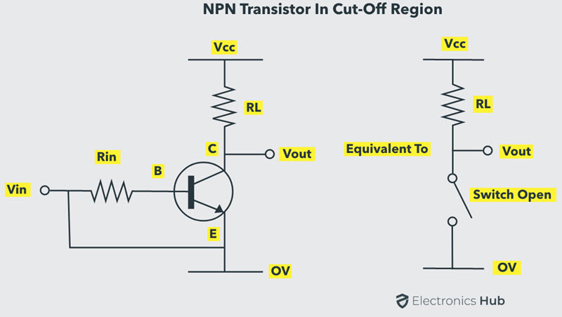
Cutoff Mode
In this mode, both collector base junction and emitter base junction are reverse biased. As both the PN Junctions are reverse biased, there is almost no current flow except small leakage currents (usually in the order of few nano amps or pico amps). BJT in this mode is switched OFF and is essentially an open circuit.
Cutoff Region is primarily used in switching and digital logic circuits.
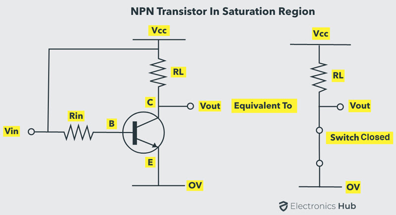
Saturation Mode
In this mode of operation, both the emitter-base and collector-base junctions are forward biased. Current flows freely from collector to emitter with almost zero resistance. In this mode, the transistor is fully switched ON and is essentially a close circuit.
Saturation Region is also primarily used in switching and digital logic circuits.
The below figure shows the output characteristics of a BJT. In the below figure, the cutoff region has the operating conditions when the output collector current is zero, zero base input current and maximum collector voltage. These parameters cause a large depletion layer, which further doesn’t allow current to flow through the transistor. Therefore, the transistor is completely in OFF condition.
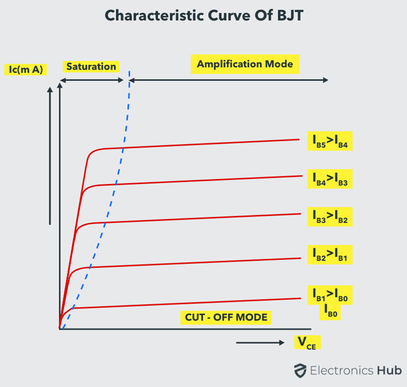
Similarly, in the saturation region, a transistor is biased in such a way that maximum base current is applied that results in maximum collector current and minimum collector-emitter voltage. This causes the depletion layer to become small and to allow maximum current flow through the transistor. Therefore, the transistor is fully in ON condition.
Hence, from the above discussion, we can say that transistors can be made to work as ON/OFF solid-state switch by operating transistor in cutoff and saturation regions. This type of switching application is used for controlling LEDs, motors, lamps, solenoids, etc.
Transistor as a Switch
A transistor can be used for switching operation for opening or closing of a circuit. This type solid state switching offers significant reliability and lower cost when compared to conventional relays.
Both NPN and PNP transistors can be used as switches. Some of the applications use a power transistor as switching device, at that time it may necessary to use another signal level transistor to drive the high-power transistor.
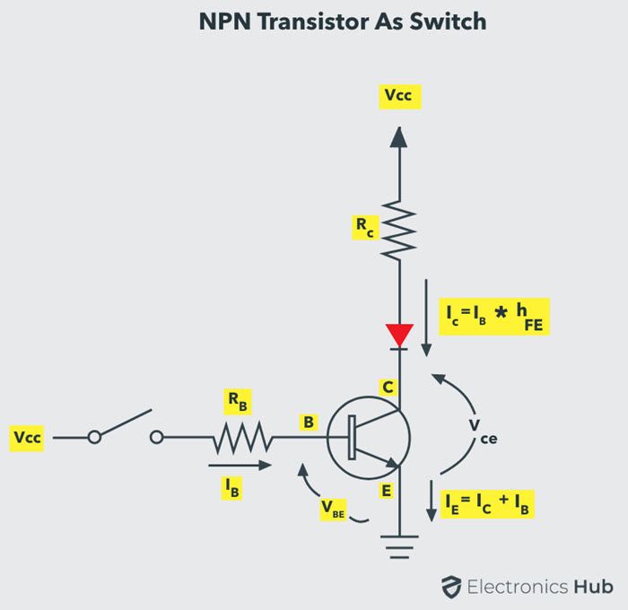
NPN Transistor as a Switch
Based on the voltage applied at the base terminal of a transistor switching operation is performed. When a sufficient voltage (VIN > 0.7 V) is applied between the base and emitter, collector to emitter voltage is approximately equal to 0. Therefore, the transistor acts as a short circuit. The collector current VCC / RC flows through the transistor.
Similarly, when no voltage or zero voltage is applied at the input, transistor operates in cutoff region and acts as an open circuit. In this type of switching connection, load (here an LED is used as a load) is connected to the switching output with a reference point. Thus, when the transistor is switched ON, current will flow from source to ground through the load.
Example of NPN Transistor as a Switch
Consider the below example, where base resistance RB = 50 KΩ, collector resistance RC = 0.7 KΩ, VCC is 5V and the beta value is 125. At the base, an input signal varying between 0V and 5V is given. We are going to see the output at the collector by varying the VI at two states that is 0 and 5V as shown in figure.
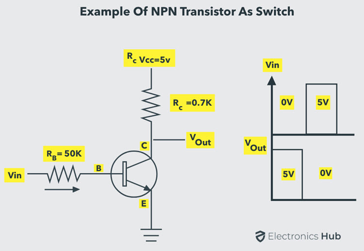
IC = VCC / RC, when VCE = 0
IC = 5V / 0.7 KΩ
IC = 7.1 mA
Base Current IB = IC / β
IB = 7.1 mA / 125
IB = 56.8 µA
From the above calculations, the maximum or peak value of the collector current in the circuit is 7.1mA when VCE is equal to zero. And the corresponding base current for this collector current is 56.8 µA.
So, it is clear that when the base current is increased beyond the 56.8 micro ampere, then the transistor comes into the saturation mode.
Consider the case when zero volt is applied at the input. This causes the base current to be zero and as the emitter is grounded, emitter base junction is not forward biased. Therefore, the transistor is in OFF condition and the collector output voltage is equal to 5V.
When VI = 0V, IB = 0 and IC =0,
VC = VCC – (IC * RC)
= 5V – 0
= 5V
Consider that input voltage applied is 5 volts, then the base current can be determined by applying Kirchhoff’s voltage law.
When VI = 5V,
IB = (VI – VBE) / RB
For silicon transistor, VBE = 0.7 V
Thus, IB = (5V – 0.7V) / 50 KΩ
= 86 µA, which is greater than 56.8 µA
Therefore, as the base current is greater than 56.8 micro ampere current, the transistor will be driven to saturation i.e., it is fully ON, when 5V is applied at the input. Thus, the output at the collector becomes approximately zero.
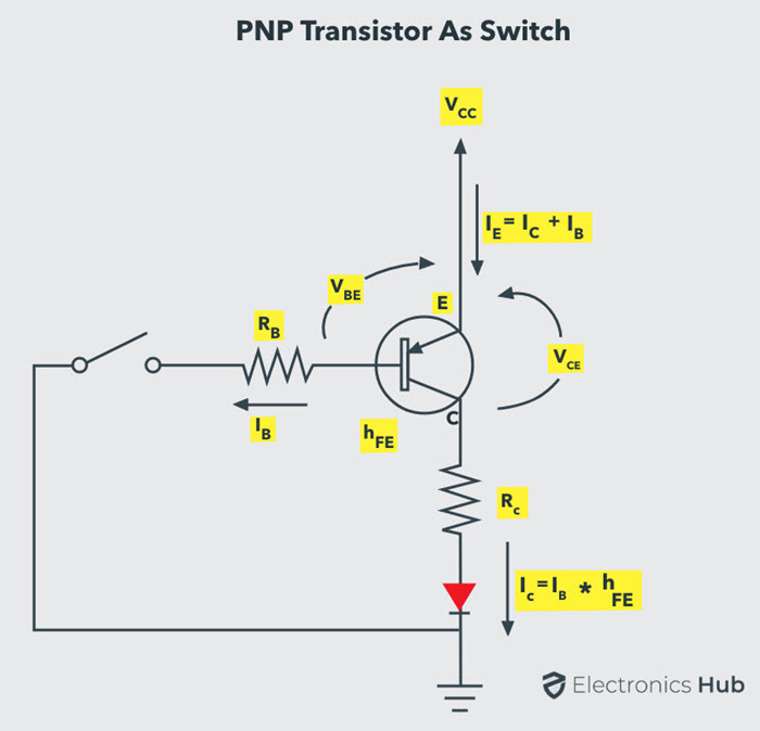
PNP Transistor as a Switch
PNP transistor works same as NPN for a switching operation, but the current flows from the base. This type of switching is used for negative ground configurations. For the PNP transistor, the base terminal is always negatively biased with respect to the emitter.
In this switching, base current flows when the base voltage is more negative. Simply, a low voltage or more negative voltage makes the transistor to short circuit otherwise, it will be open circuit.
In this connection, load is connected to the transistor switching output with a reference point. When the transistor is turned ON, current flows from the source through transistor to the load and finally to the ground.
Example of PNP Transistor as a Switch
Similar to the NPN transistor switch circuit, PNP circuit input is also base, but the emitter is connected to constant voltage and the collector is connected to ground through the load as shown in figure.
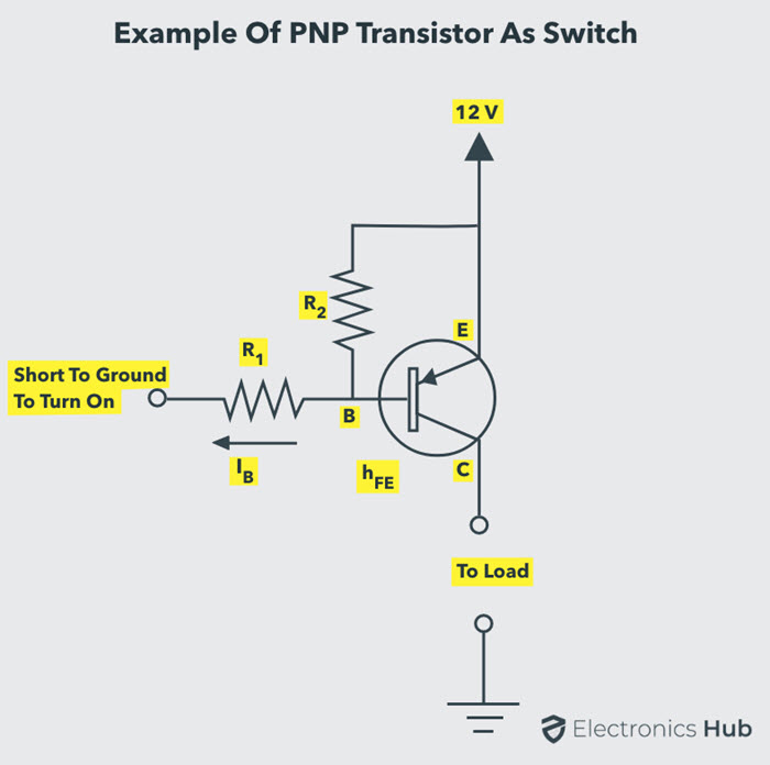
In this configuration, base is always biased negatively with respect to the emitter by connecting the base at negative side and the emitter at the positive side of the input supply. So, the voltage VBE is negative and the emitter supply voltage with respect to the Collector is positive (VCE positive).
Therefore, for the conduction of transistor emitter must be more positive with respect to both collector and base. In other words, base must be more negative with respect to the emitter.
For calculating the base and collector currents following expressions are used.
IC = IE – IB
IC = β * IB
IB = IC / β
Consider the above example, that the load requires 100 milli ampere current and the transistor has the beta value of 100. Then the current required for the saturation of the transistor is
Minimum base current = collector current / β
= 100 mA / 100
= 1mA
Therefore, when the base current is 1 mA, the transistor will be fully ON. But practically 30 percent of more current is required for guaranteed saturation of transistor. So, in this example the base current required is 1.3mA.
Practical Examples of Transistor as a Switch
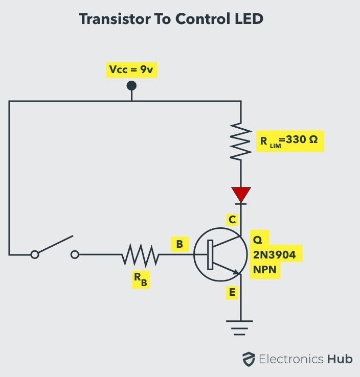
Transistor to Switch the LED
As discussed earlier, the transistor can be used as a switch. The schematic below shows how a transistor is used to switch the Light Emitting Diode (LED).
- When the switch at the base terminal is open, no current flows through the base so the transistor is in the cutoff state. Therefore, the transistor acts as an open-circuit and the LED becomes OFF.
- When the switch is closed, base current starts flowing through the transistor and then drives into saturation, which results in LED to turn ON.
- Resistors are placed to limit the currents through the base and LED. It is also possible to vary the intensity of LED by varying the resistance in the base current path.
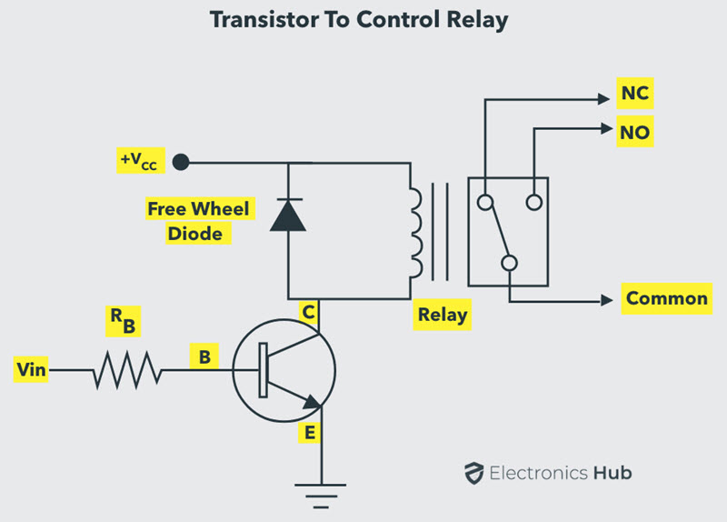
Transistor to Operate the Relay
It is also possible to control the relay operation using a transistor. With a small circuit arrangement of a transistor able to energize the coil of the relay so that the external load connected to it is controlled.
- Consider the below circuit to know the operation of a transistor to energize the relay coil. The input applied at the base causes to drive the transistor into saturation region, which further results the circuit becomes short circuit. So, the relay coil gets energized and relay contacts get operated.
- In inductive loads, particularly switching of motors and inductors, sudden removal of power can keep a high potential across the coil. This high voltage can cause considerable damage to the rest circuit. Therefore, we have to use the diode in parallel with inductive load to protect the circuit from induced voltages of the inductive load.
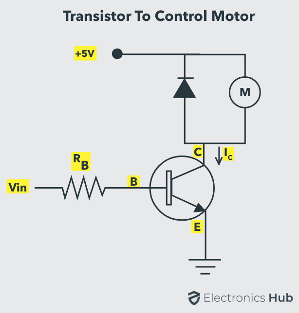
Transistor to Drive the Motor
- A transistor can also be used to drive and regulate the speed of the DC motor in a unidirectional way by switching the transistor in regular intervals of time as shown in the below figure.
- As mentioned above, the DC motor is also an inductive load so we have to place a freewheeling diode across it to protect the circuit.
- By switching the transistor in cutoff and saturation regions, we can turn ON and OFF the motor repeatedly.
- It is also possible to regulate the speed of the motor from standstill to full speed by switching the transistor at variable frequencies. We can get the switching frequency from control device or IC like microcontroller.
Have you got the clear idea of how a transistor can be used as a switch? We hope that the furnished information with relevant images and examples clarifies the entire Transistor switching concept. Further, if you have any doubts, suggestions and comments, you can write below.
Conclusion
A complete tutorial on using Transistor as a Switch. Learn the basics of Bipolar Junction Transistor, regions of operation of a Transistor, working of NPN and PNP Transistors as Switch, practical application of switching transistor.

16 Responses
Great tutorial. Thanks a lot.
Very nice explaination. It can be better if you use animated ckt.
thanx a lot …??
?????
Very good explanation.thank you
sir can u help for biasing of mosfet. i need notes for this topic.
yeah I have it
So..proper and exact explanation… Thanks a lot sr
Really great explntn
Nice explanation …
Informative website. Helps to understand
Loved a lot….
More n more information given in this I have not understood when my teacher explained but I understood when I red it once tx for this info……
Too helpfull
Very good explanation……???
Sir very Useful article and very good explanation thanks sir
Got the subject and need more information
O was really stuck on transistors for almost 2 months, studying class notes but got nothing. Today I made it.Thanks sir???
Perfect explanation on this topic. Thank you