In this tutorial, we will learn about Summing Amplifier, its configurations, types of summing amplifiers (inverting and non-inverting) and a few applications of Summing Amplifier.
One of the important applications of an Operational Amplifier is the Summing Amplifier otherwise known as Adder. As the name suggests, a Summing Amplifier is an Op-amp based circuit where multiple input signals of different voltages are added.
For information on the basics of Op-amp, read Operational Amplifier Basics.
What is Summing Amplifier?
Many applications in electronic circuits require two or more analog signals to be added or combined into a single signal. One of best examples for such requirement is the Music Recording and Broadcasting applications. In case of a typical music recoding setup, it has several inputs from a number of microphones and yet the output is stereo (left and right).
This is where the Summing Amplifier comes handy, as it combines several inputs into one common signal without noise or interference. For this reason, the Summing Amplifier is also called as Voltage Adder as its output is the addition of voltages present at its input terminal.
Inverting Summing Amplifier
The most commonly used Summing Amplifier is an extended version of the Inverting Amplifier configuration i.e., multiple inputs are applied to the inverting input terminal of the Op Amp, while the non-inverting input terminal is connected to ground. Due to this configuration, the output of Voltage Adder circuit is out of phase by 180o with respect to the input.
A general design of the Summing Amplifier is shown in the following circuit. Normal Inverting Amplifier circuit has only one voltage / input at its inverting input terminal. If more input voltages are connected to the inverting input terminal as shown, the resulting output will be the sum of all the input voltages applied, but inverted.
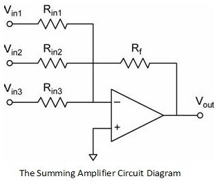
Before analyzing the above circuit, let us discuss about an important point in this setup: The concept of Virtual Ground. As the Non-Inverting Input of the above circuit is connected to ground, the Inverting Input terminal of the Op Amp is at virtual ground. As a result, the inverting input node becomes an ideal node for summing the input currents.
The circuit diagram of a summing amplifier is as shown in the figure above. Instead of using a single input resistor, all the input sources have their own input drive resistors. A circuit like this amplifies each input signal. The gain for each input is given by the ratio of the feedback resistor Rf to the input resistance in the respective branch.
Inverting Summing Amplifier Output Voltage Calculation
Let R1 be the input impedance and V1 be the input voltage of the first channel. Similarly, R2 – V2 for second channel, R3 – V3 for third channel and so on up to Rn – Vn for nth channel.
It is already been said that a summing amplifier is basically an Inverting Amplifier with more than one voltage at the inverting input terminal. The output voltage for each channel can be calculated individually and the final output voltage will be the sum of all the individual outputs.
To calculate the output voltage of a particular channel, we have to ground all the remaining channels and use the basic inverting amplifier output voltage formula for each channel.
If all the channels are grounded except the first channel, then output for first channel is given by:
VOUT1 = – (Rf / R1) V1
Where, – (Rf / R1) is the voltage gain for first channel (AV1).
Similarly, if all the channels are grounded except the second channel, then output for second channel is given by:
VOUT2 = – (Rf / R2) V2
Where, – (Rf / R2) is the voltage gain for second channel (AV2).
Likewise, the output for nth channel is given by:
VOUTn = – (Rf / Rn) Vn
And – (Rf / Rn) is the voltage gain for nth channel (AVn).
The output signal is the algebraic sum of individual outputs or in other words it is the sum of all the inputs multiplied by their respective gains.
VOUT = VOUT1 + VOUT2 + . . . + VOUTn
VOUT = – [(Rf / R1) V1 + (Rf / R2) V2 + . . . + (Rf / Rn) Vn]
VOUT = V1 AV1 + V2 AV2 + . . . + Vn AVn
In a summing amplifier, if the input resistances are not equal, the circuit is called a Scaling Summing Amplifier. But if all the input resistances are chosen to be of equal magnitude, then the Summing Amplifier is said to be having an equal-weighted configuration, where the gain for each input channel is same.
Sometimes, it is necessary to just add the input voltages without amplifying them. In such situations, the value of input resistance R1, R2, R3 etc. must be chosen equal to that of the feedback resistor Rf. As a result, the gain of the amplifier will be unity. Hence, the output voltage will be an addition of the input voltages.
Theoretically, we can apply as many input signals to the input of the summing amplifier as required. However, it must be noted that all of the input currents are added and then fed back through the resistor Rf, so we should be aware of the power rating of the resistors.
Non-Inverting Summing Amplifier
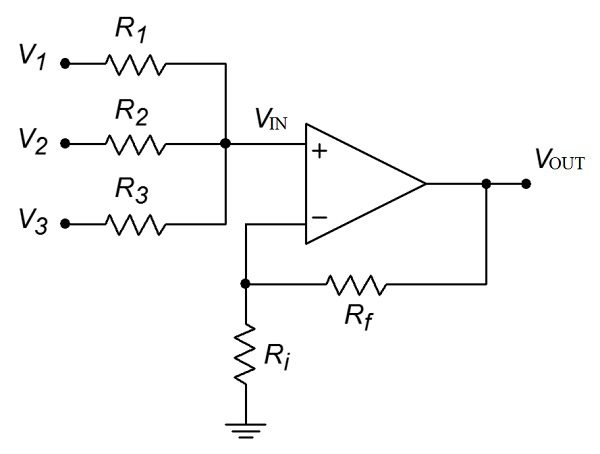
A Non-Inverting Summing Amplifier can also be constructed using the Non-Inverting Amplifier configuration of the Op Amp. Here, the input voltages are applied to the non-inverting input terminal of the Op Amp and a part of the output is fed back to the inverting input terminal, through voltage-divider-bias feedback.
The circuit of a Non-Inverting Summing Amplifier is shown in the following image. For the sake of convenience, the following circuit consists of only three inputs, but more inputs can be added.
First and foremost, even though this is also a Summing Amplifier, the calculations are not as straight forward as the Inverting Summing Amplifier because there is no advantage of virtual ground summing node in the Non-Inverting Summing Amplifier.
Non-Inverting Summing Amplifier Output Voltage Calculation
To understand the working of a Non-Inverting Summing Amplifier, we have to divide the circuit into two parts:
- Input Resistor / Source Section
- Non-Inverting Amplifier Section
If VIN is the combination of all the input signals, then this is applied at the non-inverting terminal of the Op Amp. From the above circuit, we can calculate the output voltage of the Non-Inverting Amplifier with VIN as input and Rf and Ri as the feedback divider resistors as follows:
VOUT = VIN (1 + (Rf / Ri))
As the output voltage is figured out, we have to now determine the value of VIN. If V1, V2 and V3 are the three main input sources and R1, R2 and R3 are their input resistances, then VIN1, VIN2 and VIN3 are the inputs of respective channels when other corresponding channels are grounded. So,
VIN = VIN1 + VIN2 + VIN3
As the concept of virtual ground doesn’t apply here, all channels will have an effect on other channels. Let us calculate the VIN1 portion of the VIN and by simple mathematics, we can easily derive the other two values i.e., VIN2 and VIN3.
Coming to VIN1, when V2 and V3 are grounded, their corresponding resistors cannot be ignored as form a voltage divider network. So,
VIN1 = V1 [(R2 || R3) / (R1 + (R2 || R3))]
Similarly, we can calculate the other two values VIN2 and VIN3 as
VIN2 = V2 [(R1 || R3) / (R2 + (R1 || R3))]
VIN3 = V3 [(R1 || R2) / (R3 + (R1 || R2))]
So,
VIN = VIN1 + VIN2 + VIN3
VIN = V1 [(R2 || R3) / (R1 + (R2 || R3))] + V2 [(R1 || R3) / (R2 + (R1 || R3))] + V3 [(R1 || R2) / (R3 + (R1 || R2))]
Finally, we can calculate the Output voltage VOUT as
VOUT = VIN (1 + (Rf / Ri))
VOUT = (1 + (Rf / Ri)) {V1 [(R2 || R3) / (R1 + (R2 || R3))] + V2 [(R1 || R3) / (R2 + (R1 || R3))] + V3 [(R1 || R2) / (R3 + (R1 || R2))]}
If we consider the special equal weighted condition where all the resistors are having the same values, then the output voltage is:
VOUT = (1 + (Rf / Ri)) ( (V1 + V2 + V3) / 3)
Design of non-inverting summing circuit is approached by first designing the non-inverting amplifier to have the required voltage gain. Then the input resistors are selected as large as possible to suit the type of the op-amp used.
Voltage Adder Example
Three audio signals drive a summing amplifier as shown in the following circuit. What is the output voltage?
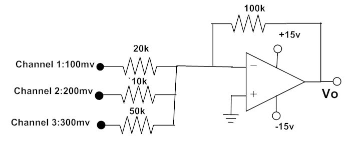
The closed loop voltage gains of each channel can be calculated as:
ACL1 = – (Rf / R1) = – (100 KΩ / 20 KΩ) = – 5
ACL2 = – (Rf / R2) = – (100 KΩ / 10 KΩ) => ACL2 = – 10
ACL3 = – (Rf / R3) = – (100 KΩ / 50 KΩ) => ACL3 = – 2
The output voltage of the summing amplifier is given as,
VOUT = (ACL1 V1 + ACL2 V1 + ACL3 V1)
= – [(5 * 100 mV) + (10 * 200 mV) + (2 * 300 mV)]
= – (0.5 V + 2 V + 0.6 V)
VOUT = – 3.1 V
Summing Amplifier Applications
Audio Mixer
A summing amplifier is a useful circuit when two or more signals need be added or combined, like in audio mixing applications. The sounds from different musical instruments can be converted to a specific voltage level, using transducers, and connected as input to a summing amplifier.
These different signal sources will be combined together by the summing amplifier and the combined signal is sent to an audio amplifier. An example circuit diagram of a summing amplifier as audio mixer is shown in the figure below.
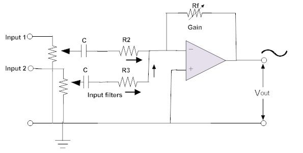
The summing amplifier can function as a multi-channel audio mixer for several audio channels. No interference (feedback from one channel to the input of another channel) will occur because each signal is applied through a resistor, with its other end connected to ground terminal.
Digital to Analog Converter (DAC)
A Digital to Analog Converter (DAC) converts the binary data applied to its input into an equivalent analog voltage value. Real-time industrial control applications often use microcomputers. These microcomputers output digital data needs to be converted to an analog voltage to drive the motors, relays, actuators, etc.
The simplest Digital to Analog Converter circuit uses a summing amplifier and a weighted resistor network. A typical 4-bit DAC circuit using a summing amplifier is shown in the below figure.
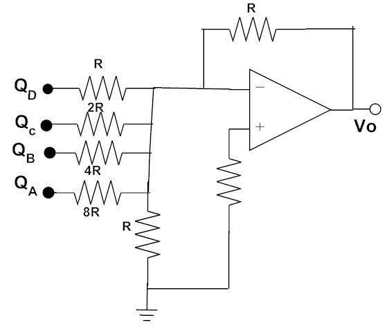
The inputs to the above shown summing amplifier are the binary data QA, QB, QC and QD, which are usually 5 V to represent logic 1 and 0 V to represent logic 0.
If the input resistors in each branch are chosen in such that the value of each input resistor is double the value of the resistor in previous input branch, then a digital logical voltage at the input will produce an output which is a weighted sum of the input voltages applied.
The accuracy of such a digital to analogue converter circuit is limited by the accuracy of the resistor values employed and the variations in representing the logic levels.
Level Shifter
Another important application of a Summing Amplifier is a Level Shifter. A 2-input Summing Amplifier can act as a level shifter, where one input is an AC Signal and the second input is a DC Signal.
The AC Signal will be offset by the input DC Signal. One of the major applications of such level shifter is in Signal Generators for DC Offset Control.
Conclusion
A complete beginner’s tutorial on Summing Amplifiers or otherwise known as Adder Circuits. You learned some basics of Summing Amplifier, Inverting and Non-Inverting Summing Amplifier, output voltage calculation, an example circuit and few important applications.

2 Responses
The OpAmp in the non inverting circuit example is flipped regarding input + and –
yes you’re right thank you