Voltage Multipliers, as the name suggests, are circuits that multiply the input voltage by a factor of two, three or higher. Commonly used Voltage Multipliers are Voltage Doubler, Voltage Tripler and Voltage Quadruple circuits.
Voltage Multipliers are also rectifiers that convert AC to DC, but multiply the voltage. In case of a Voltage Doubler Circuit, if the input voltage is 12V, the output voltage will be approximately 24V.
Even though step up transformers in combination with rectifier circuit can be used to generate high voltage DC, this setup requires a bulky transformer at mains and the peak inverse voltage (PIV) of the rectifier diode must be high.
Hence, step up transformers are used in applications where high voltage and high current is required whereas Voltage Multipliers like Voltage Doublers and Voltage Triplers are used in applications where high voltage and low current is required.
Voltage Doubler and Voltage Tripler Circuits
In this project, we have designed a simple Voltage Doubler Circuit using 555 Timer. Additionally, we have also designed a transformer based Voltage Doubler and Voltage Tripler.
Circuit of Voltage Doubler using 555

Components Required
- IC 555
- 22 µF / 50V Electrolytic Capacitor x 2
- 1N4007 PN Junction Diode x 2
- 100 nF Ceramic Capacitor (Capacitor Code – 104)
- 1 nF Ceramic Capacitor (Capacitor Code – 102)
- 30 KΩ Resistor (1/4 Watt)
- Power Supply
- Breadboard
- Connecting Wires
- Multimeter (for checking input and output voltage)
Circuit Design
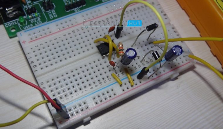
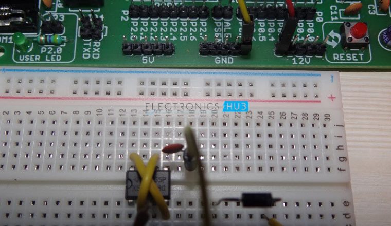
555 Timer is used as an Astable Multivibrator. Pins 4 and 8 (RESET and VCC) are connected to VCC and Pin 1 is connected to GND. Pins 2 and 6 (TR and TH) are shorted. A 1 nF capacitor (C3) is connected between pin 2 and GND.
A 100 nF capacitor (C4) is connected between pin 5 and GND. A 30 KΩ Resistor is connected between pins 3 and 2. This completes the High Frequency Pulse i.e. Astable Multivibrator part of the circuit.
The Voltage Doubler part consists of two 22 µF Capacitors and two 1N4007 PN Junction Diodes. The voltage rating of the Capacitor is an important factor and it must be more that the output voltage.
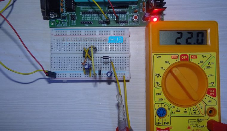
Since we intend to supply an input voltage of 12V, the output voltage will not be greater than 24V. So, the voltage rating of the two 22 µF Capacitors we chosen at 50V.
Working of Voltage Doubler using 555
The output of the 555 Timer is a square wave of approximately 50% Duty Cycle and a frequency of approximately 23 KHz. When the output of the 555 Timer at Pin 3 becomes LOW, Diode D1 becomes forward biased. As a result, the Capacitor C1 gets charged to the supply voltage through D1.
When the output of the 555 Timer at Pin 3 goes HIGH, Diode D1 gets reverse biased and doesn’t allow the Capacitor C1 to discharge. At the same time, Diode D2 gets forward biased and allows charging of Capacitor C2. C2 charges to a combination of supply voltage and voltage stored in the Capacitor C1 (which is equal to supply voltage). Hence, the voltage across Capacitor C2 will be twice the supply voltage.
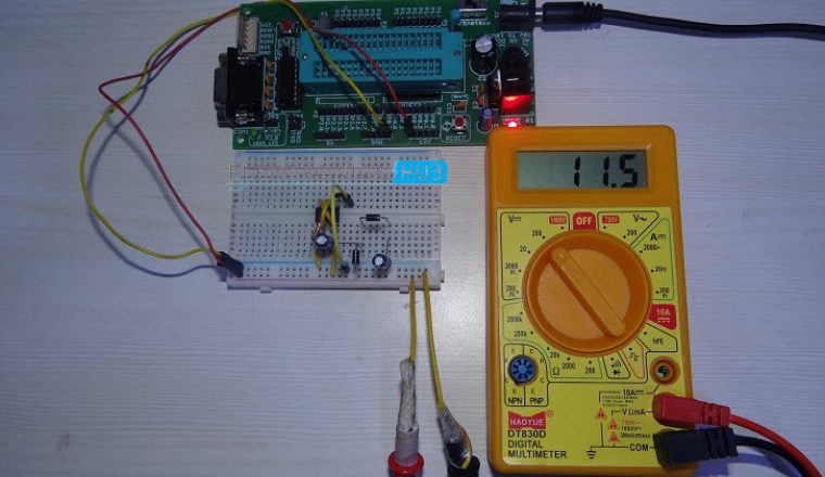
Theoretically, the voltage across C2 should be double that of the VCC (supply voltage) but practically, this voltage will be slightly less than that. For example, during our practical testing, we have supplied with two different voltages of 8.6 V and 11.8 V. The output voltages were 14.8 V and 22.5 V respectively.
Voltage Tripler Circuit
Voltage Tripler is another Voltage Multiplier Circuit, where the output voltage is three times that of the input voltage i.e. if the input voltage is 9V, the output voltage will be 27 V (approximately). For the Voltage Tripler Circuit, we implemented a transformer based design as follows.
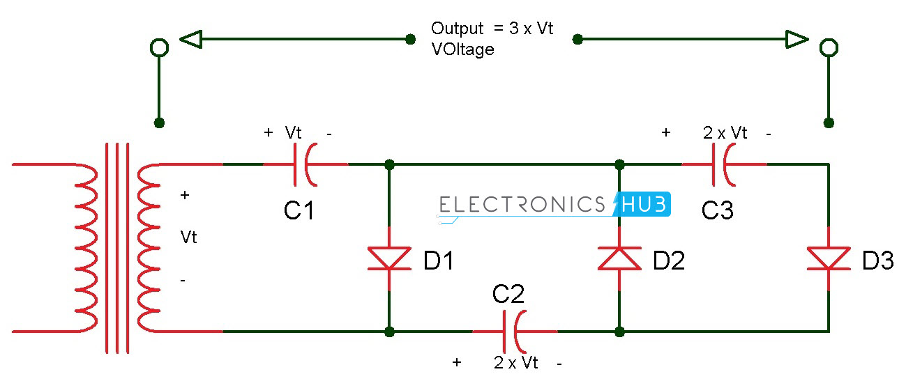
Working of Voltage Tripler Circuit
Let the voltage across the secondary of the transformer be Vt Sinwt. During the positive cycle, diode D1 id forward biased and allows the capacitor C1 to charge to peak of Vt Sinwt i.e. Vt. During this time, the diodes D2 and D3 are reverse biased.
During the negative cycle, diode D2 is forward biased and allows the Capacitor C2 to charge. As the voltage across the capacitor C1 and the secondary of the transformer are additive in nature, the capacitor C2 will charge to 2Vt.
During the next positive cycle, capacitor C1 holds its charge at Vt and hence the diode D1 cannot conduct. Assuming the C3 is initially uncharged, the conduction path for this positive cycle will be Capacitor C1, Capacitor C3, Diode D3 and Capacitor C2.
Since D3 is forward biased, capacitor C3 will charge to 2Vt, which is the sum of transformer’s secondary and voltage across Capacitor C1. If the voltage is taken across Capacitors C1 and C3, the voltage will be the sum across the individual capacitors i.e. Vt + 2Vt = 3Vt. Hence, the circuit acts as a Voltage Tripler.
Voltage Quadrupler Circuit
From the Voltage Tripler Circuit, it is clear that the voltage across Capacitor C2 is two times the secondary voltage i.e. that part of the circuit acts as Voltage Doubler Circuit.
Similarly, we can build a Voltage Quadrupler Circuit by adding a Capacitor and Diode to the Voltage Tripler Circuit. The following image shows the circuit of a Voltage Quadrupler.

Working of Voltage Quadrupler Circuit
The part until Capacitor C3 and Diode C3 is similar to that of Voltage Tripler. By applying the same principle of positive cycle and negative cycle of Voltage Tripler Circuit to the Voltage Quadrupler Circuit, we can easily understand that during the second negative cycle, the Diode D4 conducts and the voltage across Capacitor C4 will be 2Vt.
By taking the voltage across capacitors C2 and C4, we get the output voltage of four times the secondary transformers’ voltage. Hence, the above circuit acts as a Voltage Quadrupler.
NOTE: In the Voltage Quadrupler Circuit, we have marked the points for Voltage Doubler and Voltage Tripler respectively.
Points to Remember
- The first Voltage Doubler Circuit using 555 is a low current circuit. The output current is very less (few milli Amperes).
- The peak inverse voltage (PIV) of the diodes used in Voltage Tripler and Voltage Quadrupler Circuit must be rated at 2Vt.
- Also, the capacitors must be large and rated with proper voltages.
- More than four stages i.e. Voltage Quadrupler is not very practical as the number of diode – capacitor pairs increases, the final capacitors may not be charges to the secondary voltage.

One Response
I want voltage triper conclusion……