Switch Mode or Switching Mode Power Supply or simply SMPS is a type of Power Supply Unit (PSU) that uses some kind of switching devices to transfer electrical energy from source to load. Usually the source is either AC or DC and the load is DC.
The most common application of an SMPS is the power supply unit of a computer. Switching Mode Power Supply (SMPS) has become a standard type of power supply unit for electronic devices because of their high efficiency, low cost and high power density.
Switch Mode Power Supply (SMPS)
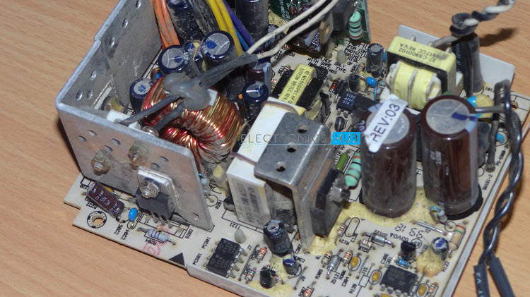
The following image shows an SMPS unit from an old desktop computer. This particular SMPS is rated for 90W of power.
Linear Regulator vs. SMPS
A Power Supply Unit is an important part of an electric circuit as it provides the power to the circuit for a proper operation. Almost all electronic devices require a constant voltage without any fluctuations. A power supply will take an unregulated power and converts it into a stable regulated power. There are basically two categories of Power Supplies: Linear Regulated Power Supply and Switching Mode Power Supply (SMPS).
Linear Regulated Power Supply is a type of power supply that regulates the output voltage with the help of a series pass control element. The basic example of a series pass element is a resistor. But the frequently used series pass elements are BJT or MOSFET in active or Linear Mode and is connected in series with the load.
Depending on the changes in either input or load, the current through the transistor changes in order to keep the output constant. The difference between the input and output (load) voltages is dropped across the transistor and this excess power i.e. difference between the input and output (load) power is dissipated as heat by the transistor.
The following image shows a basic structure of a Linear Regulated Power Supply.
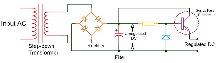
From the above image, the input AC source is given to a rectifier and filter to convert it into DC. But this DC Supply is unregulated as it is susceptible to change with the changes in input. This unregulated DC supply is given as input to the Linear Regulator.
SMPS is a type of regulated power supply that uses a high frequency switching regulator to convert the power supply and also regulate the output in a highly efficient way.
The switching regulator is again a transistor (like a power MOSFET) just like in Linear Regulator but the difference is that the pass transistor in SMPS doesn’t continuously stay in saturation or fully ON state but rather switches between fully ON and fully OFF states at a very high frequency. Hence the name Switching Mode Power Supply.
Since the average time the switching element i.e. the transistor stays in active state is less, the amount of power wasted or dissipated as heat is very less when compared to Linear Regulators. This in turn leads to high efficiency of SMPS as the voltage drop across the pass transistor (or switching element) is very less.
The switching action of the transistor is controlled using a technique called Pulse Width Modulation (PWM) and the output voltage can be regulated by the duty cycle of the PWM.
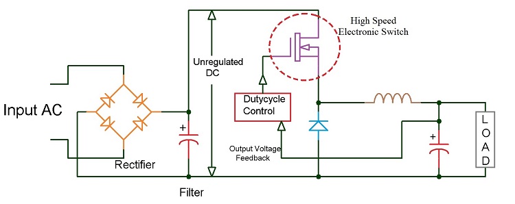
The above image shows a basic structure of an SMPS unit. In this, the unregulated DC supply is given to a Switched Mode DC – to – DC Chopper Circuit and the output is a regulated DC Supply.
The main difference between the structures of Linear Regulated Power supply and Switch Mode Power Supply shown here is that in case of Linear Power Supply, the input AC is stepped down, rectified and filtered to get unregulated DC and in case of SMPS, the input AC is directly rectified and filtered and the unregulated high voltage DC is given to a High Frequency DC – to – DC Converter.
Usually, a high frequency transformer will be a part of this DC – to – DC converter for scaling and isolation.
Specification
Linear
SMPS
Efficiency
Typical efficiency of 30-40%
Typical efficiency of 60-95% can be achieved with good design
Output Voltage
Always less than Input
Can be more or less than Input
Regulation Method
By dissipating excess power
By varying duty cycle of PWM
Circuit Complexity
Less complex; consists of regulator and filter as main components
Very complex; consists of switching element, high frequency transformer, rectifiers and filters, feedback circuit
Noise and Interference
Less electronic noise at output and mild high frequency interference
High interference and noise due to frequent switching od current
Size and weight
Bulky because of transformer and heat sink
No transformer at input but requires a tiny high frequency transformer
Applications
Low power, simple and low cost systems
High power, complex and stable power requirements
Even though the design of Switch Mode Power Supply (SMPS) is more complex than a Linear Regulated Power Supply, its high efficiency, high power capabilities and stability are the main factors in choosing SMPS as the power supply unit for sensitive electronic devices.
What is the purpose of SMPS?
Majority of Electronic DC Loads like Microprocessors, Microcontrollers, LEDs, Transistors, ICs, Motors etc. are supplied with standard power sources like batteries for example. Unfortunately, the prime problem with batteries is the voltage is either too high or too low. Hence, an SMPS will provide a regulated DC output.
SMPS is a versatile power supply as we can choose from different topologies like Step – up (Boost), Step – down (Buck), power supplies with isolation at input and output depending on the type of application.
Coming to the major factor of why we need SMPS, the efficiency of a good SMPS design can be as high as 90% or even more. In contrast, the efficiency of a Linear Regulated Power Supply is dependent on the voltage drop at the pass transistor.
For example, assume we have a 3V Lithium Cell that must be stepped down to a 1.8V load drawing a current of 100mA. The power wasted in the transistor as heat is 0.12W and hence the efficiency of the power supply is 40%.
SMPS ICs come with more or less all the features of a discrete SMPS design allowing engineers to experiment with design for custom projects.
SMPS Design
The design of Switched Mode Power Supply or SMPS is fairly complex when compared to linear regulated power supply. But this complexity in design has an advantage as it will result in stable and regulated DC supply that is capable of delivering more power in an efficient way for a given physical specification (size, weight and cost).
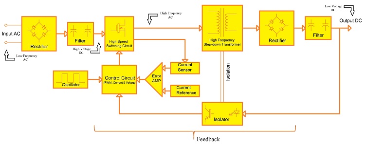
A simplified block diagram of an SMPS which converts AC input to a regulated DC is shown in the following image.
Although there are many number of design types for an SMPS power supply, all the designs will be more or less similar to the structure shown above. The main design types in SMPS are:
- AC to DC, where AC mains is given as input and we get a regulated DC at the output,
- DC to DC Step up converter, where an input DC voltage is stepped up i.e. output voltage is greater than input and
- DC to DC Step down converter, where the input DC voltage is stepped down i.e. output voltage is less than or equal to input voltage.
In case of DC to DC SMPS systems, the input DC is usually given from a battery and hence, both the DC to DC converter circuits (Step up and Step down) are commonly found in battery operated systems.
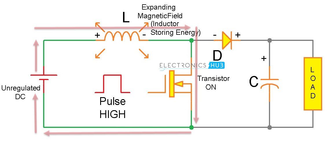
Coming back to SMPS design in the above image, it represents a typical AC to DC converter. We will see the basic working of this SMPS design. The input AC supply is given to rectifier and filter circuits. This step will convert the High Voltage AC to High Voltage DC.
This high voltage DC is given to a High Speed Switching Element like a Power MOSFET. The output of this switch, which is a High Frequency, High Voltage Pulsating AC, is given to a High Frequency Step down Transformer.
The output of this transformer is a Low Voltage AC signal which is in turn given to a rectifier and a filter circuit to obtain Low Voltage DC.
Important Points to Note:
- The common feature of any SMPS design is to convert input AC to High Voltage DC and convert this High Voltage DC to High Voltage, High Frequency Square Wave (AC). This High Voltage and Frequency AC is converted to Regulated DC.
- Square Wave Oscillator and High Speed Electronic Switch (like a MOSFET) are responsible for converting DC to High Frequency AC. The same principle is also used in Square Wave Inverters.
- By converting the input AC or DC (after rectifying and filtering the AC) to High Frequency AC, the size and price of the components like inductors, transformers and capacitors can reduced i.e. they can be smaller and cheaper.
- As the High Frequency AC signal generated at the switch is a square wave, the output voltage can be regulated with the help of Pulse Width Modulation (PWM). There is a voltage feedback through an isolator circuit to the control circuit (which controls the PWM). With this feedback, the duty cycle of the PWM from the oscillator can be varied and hence the output is perfectly regulated without any over voltages.
- A sample current from the High Frequency AC (signal after the switch) and a reference current are compared and given to the control circuit and hence provides an over current protection.
- Also note that the output DC is completely isolated from the input mains and even the feedback signal is isolated with the help of an Opto coupler.
- Driving the Switching Transistor (MOSFET) with square wave ensures that the power dissipation is very less when compared to the Transistor being operated as a series pass transistor in Linear Regulated Power Supplies.
- Since there is a High Frequency AC Signal in the SMPS, there is a chance of high frequency harmonics and as a result, SMPS is more susceptible to RF Interference.
SMPS Topologies
We have seen the basic design of a Switched Mode Power Supply (SMPS) in the above section. Now we will see the different types or topologies of SMPS. Switched Mode Power Supplies or SMPS can be classified into two types based on its circuit topology: Non-isolated Converters and Isolated Converters.
Non – isolated Converters are a type of SMPS Topology where the switching circuit and output are not isolated i.e. they have a common terminal. The three basic and important types in Non – isolated SMPS are:
- Buck Converter or Step – down Converter
- Boost Converter or Step – up Converter
- Buck – Boost Converter
There are other non – isolated SMPS designs like Switched Capacitors, Cuk Converter and SEPIC Converter but these three types are very important. They are the simplest of SMPS designs and use a single inductor as an energy storing element and two switches, out of which one is an active switch (a Transistor – Power MOSFET) while the other can be a diode.
The output voltage can be higher (Boost or Step – up) or lower (Buck or Step – down) and can be controlled by the duty cycle of the high frequency square wave (that is applied to the switch). One main drawback of Non – isolated Topology is that the efficiency of the switches falls as the duty cycle is reduced. Isolated Topology will suit better for larger voltage changes.
Isolated Topology in SMPS uses a transformer as an isolator between the switching element and output. Depending on the transformer’s turns ratio, the output voltage can be higher or lower than the input. Transformer based SMPS topologies can be designed to generate multiple output voltage by using multiple windings at the transformer.
The energy storage element can be transformers secondary winding or a separate inductor. The two important Isolated Topology based SMPS converters are:
- Flyback Converter
- Forward Converter
Some of the other commonly used isolated SMPS topologies are Half – bridge, Full – bridge, Push – Pull, Half – Forward, Isolated Cuk, etc.
Buck Converter or Step – down Converter
Buck Converter is a type of SMPS circuit and DC to DC Converter, where the output voltage is less than input voltage. Hence, a Buck Converter is also known as a Step – down Converter.
It is one of the simplest SMPS power converter techniques and is often used in RAM, CPU, USB etc. The input DC in buck converter can be a rectified AC or a battery. A simple buck converter using two switches (one transistor and one diode) and an energy storing element (inductor) is shown in the image below.

Buck Converter Operation
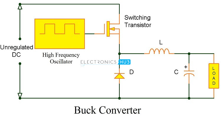
A simple Buck Converter or Step down Converter is shown in the above image and it consists of a switching transistor, diode, inductor and capacitor. The combination of Inductor , Diode and Capacitor is called as Flywheel Circuit.
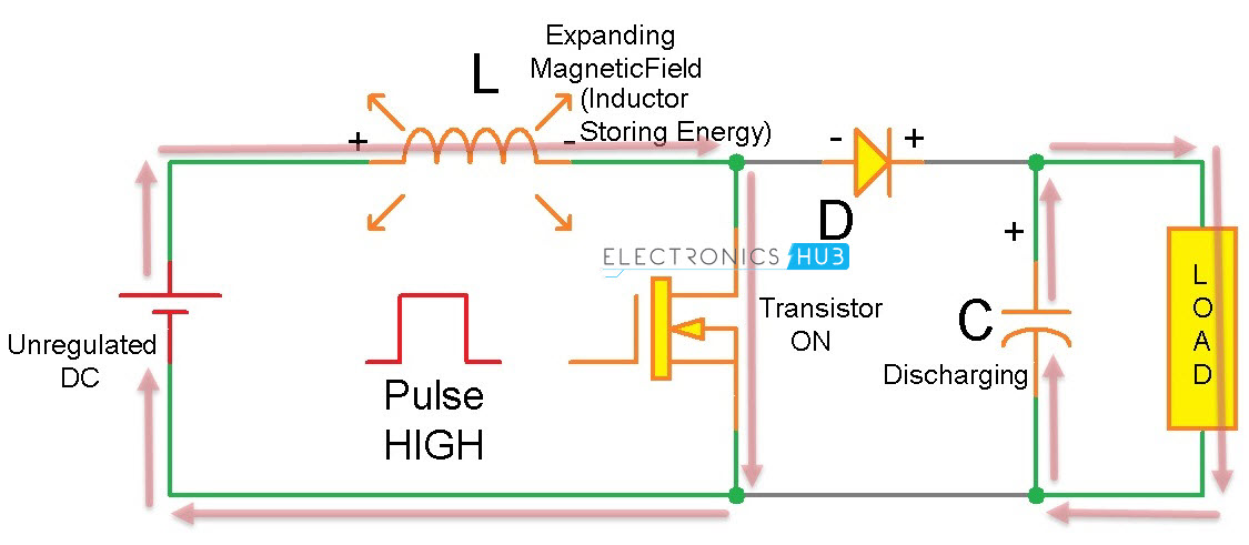
The operation of the Buck Converter is explained with respect to square wave pulse. The following image shows the operation of the Buck Converter when the input pulse is HIGH i.e. the switching Transistor is ON.
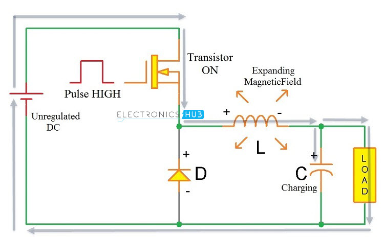
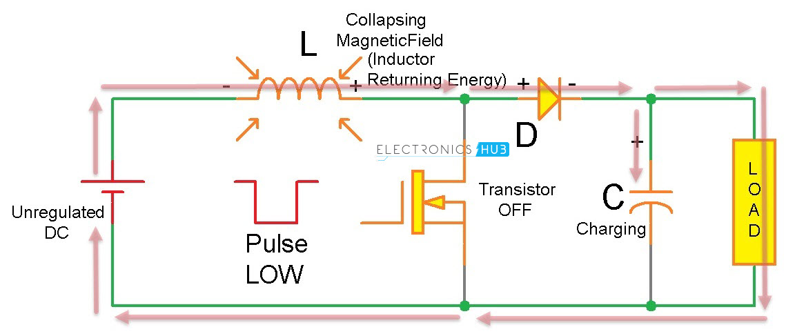
When the pulse input to the Gate terminal of the MOSFET is HIGH, the Transistor is turned ON. As a result, the transistor will supply current to the load. During this time, the Diode D is reverse biased and will not be a part of the circuit during this period.
Initially, the inductor resists the change in current and hence, the current to the load will increase gradually with expanding magnetic field. Also, the charge on the capacitor is built up gradually up to the supply voltage. The next image is for the condition where the pulse becomes LOW i.e. the Transistor is OFF.
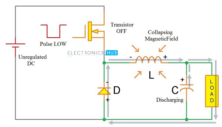
When the pulse becomes LOW, the switching Transistor is turned OFF. The magnetic field that is built up during the Transistor ON state, starts collapsing now and releases the energy back in to the circuit. The polarity of the voltage across the inductor i.e. its back e.m.f is now reversed. The energy from the inductor starts collapsing and keeps the current flowing in the circuit through load and the diode, as the diode D is forward biased.
Once the energy from the inductor is completely utilized, the capacitor starts discharging and acts as the main source of supply until the transistor is turned ON. When the transistor is turned ON, it will once again supply current to inductor, capacitor and load and the process continues.
The output voltage is dependent on the ON and OFF time i.e. the Duty Cycle of the square wave pulse and the formula for output voltage is
VOUT = D x VIN, where D = TON/(TON+TOFF)
With Buck Converters, we can achieve more than 90% efficiency and as a result, they often employed in computer systems where they convert 12V supply to typically 1.8V (for RAM, CPU and USB).
Boost Converter or Step – up Converter
In the previous section, we have seen a Buck Converter type SMPS. Now, we will see about another type of SMPS called Boost Converter or Step – up converter. A Boost Converter, as the name suggests, is type of switched mode power supply, which boosts or increases the output voltage with respect to the input voltage. Boost Converters are also known as Step – up Converters as the output voltage is higher than the input voltage.
One of the best known application for Boost Converters is in electric cars. The supply from electric cars batteries won’t be sufficient for its working as they require voltages that are much higher (typically in region of 500V) than those supplied by the batteries. Another important application of Boost Converters is Laptop Chargers in Cars.
Typical Car batteries provide 12V and Laptops require anywhere between 18 to 22V. The following image shows a simple Boost Converter.
Boost Converter Operation
This simple Boost Converter consists of a Switching Transistor (BJT or MOSFETS can be used), an energy storing element i.e. inductor, another switch (Diode or another Transistor), capacitor and a high frequency square wave oscillator with controllable duty cycle.
The input to this Boost converter is unregulated DC, which can be given from rectified AC, batteries, Solar, DC Generators, etc. We will see the working operating of this Boost Converter. First we will see for period when the Transistor is ON for the first time. The following image shows this condition.
 When the pulse is HIGH for the first time, the transistor is turned ON and it closes a part of the circuit consisting of Inductor, Transistor and input supply. Current flows from the input through the inductor and transistor.
The inductor, initially resists the change in current but the magnetic field will increase gradually allowing inductor to store energy. The impedance of the rest of the circuit i.e. Diode, Capacitor and Load is much higher and hence, there will be no flow of current in that part of the circuit.
 When the square wave pulse goes LOW, the transistor is turned OFF. This action will cause a drop in the current through the inductor, producing a back e.m.f in the circuit due to collapsing magnetic field. Also, the polarity of the voltage across the inductor is now reversed and will be in series with the input voltage.
The combination of the input voltage and Inductor Back e.m.f cannot pass through the inductor as it is turned OFF. Hence, the diode is forward biased and charges the Capacitor and also supplies current to load.
An important point to note here is that the voltage supplied to the capacitor and load during the Transistor OFF state is a combination of input voltage and inductors back e.m.f, which is higher than the input voltage.
 When the transistor is turned ON again, the current flows again through the inductor and transistor. As the diode is reverse biased, the capacitor discharges it potential, which is sum of input voltage and inductor voltage, through the load acting as its source during this period. The output voltage is given by the formula
VOUT= VIN x 1/(1-D) where D = TON/(TON+TOFF)
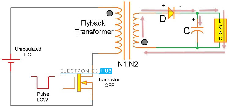
Flyback Converter
Flyback Converter is a type of Switch Mode Power Supply typically used in low power applications. Flyback Converter is an Isolated Type SMPS where the input and output are isolated with a transformer. The following is the circuit of a simple Flyback Converter.
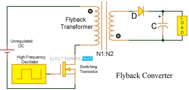
The main components of a Flyback Converter are a Switching Transistor, Oscillator Circuit, Transformer, switch (like a Diode) and a Capacitor. The Transformer is different from a normal transformer and is called a Flyback Transformer. In this transformer, the Primary and Secondary do not conduct simultaneously.
Flyback Converter Operation
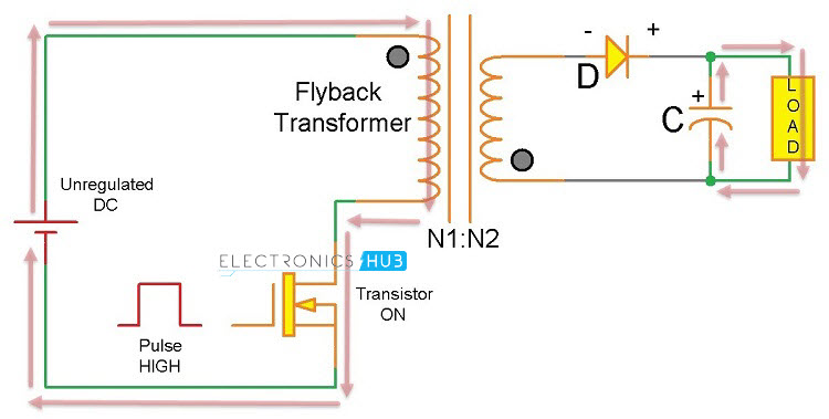
When the Transistor is turned ON, the current flows through the primary of the transformer with the dot being higher potential. As a result, the polarity of the voltage induced in the secondary will be reverse to that of primary. Hence, the diode D gets reverse biased.
If the capacitor got charged in the previous cycle, it will discharge through the load. The following image shows this period of operation in the flyback converter.
 The operation of the Flyback converter in the other period i.e. Transistor OFF period is illustrated in the following image. When the pulse becomes LOW, the transistor is turned OFF and the primary of the transformer do not conduct.
The energy in the secondary of the transformer will be released into the circuit and also the polarity in the secondary is reversed i.e. it becomes positive. Hence, the diode is forward biased allowing the energy stored in the secondary coil acting as the source. It recharges the capacitor and also supplies the current to load.
The output voltage in Flyback Converter can be higher or lower than the input voltage and is dependent on the turns ratio of the primary and secondary of the transformer.
Forward Converter
Another important switch mode power supply is Forward Converter. It is another isolated type SMPS and produces controlled and regulated DC from an unregulated DC supply.
The efficiency of Forward Converter is slightly more than that of Flyback Converter and is often used in application where the power requirements are a little higher (typically around 200W). The design of Forward Converters is slightly complex than Flyback Converters and a simple structure is shown below.
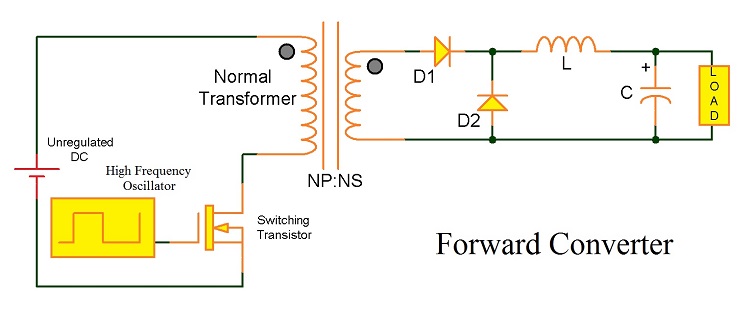
The simple circuit of Forward Converter consists of a fast switching transistor, a control circuit to control the duty cycle of the Square Wave, a normal transformer, two diodes for rectifying the AC, an inductor and a capacitor for filtering.
Forward Converter Operation
The following image shows the operation of the Forward Converter when the Transistor is turned ON. When the pulse is HIGH, the transistor is turned ON and as a result, the primary coil of the transformer starts conducting. As a result, a voltage is induced in the secondary coil of the transformer.
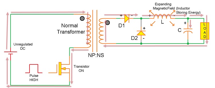
The polarity of the voltage induced in the secondary is similar to that of the primary and hence, the diode D1 gets forward biased. The voltage from the secondary will start to flow through the diode D1, inductor, capacitor and finally the load. During this period, both the inductor and capacitor store energy in the form of magnetic field and electric field respectively.
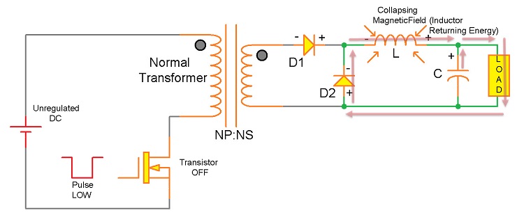
When the pulse becomes LOW, the transistor is turned OFF and as a result, the primary coil stops conducting. This will in turn stop inducing current in the secondary. This sudden change (or drop) in current will generate a back e.m.f of the inductor and polarity of its voltage is reversed.
This period of operation of the Forward Converter is shown in the image below. The energy in the inductor start collapsing in the circuit through the load and Diode D2 (as it is forward biased). As soon as the energy in the inductor finishes, the capacitor starts discharging through the load and acts as a temporary source to the load. This continues until the transistor is turned ON again
The output voltage of the Forward Converter is dependent on the transformer turns ratio as well as the duty cycle of the Pulse Width Modulator. The output voltage is given by
VOUT = VIN x D x NS/NP

10 Responses
Thank you for this excellent article. This explains the most essential facts regarding SMPS. Thank you for this awesome article.
It is perfect ,thanks
Pls i want to design cheap and simple smps convert 220v ac to 24v dc, 3a transformerless
Excellent article . The SMPS explained in a easy way for anyone who like to know.
very good article.it is help full information
This has been a very helpful article. I am great full that time was taken to compile this for people like myself that need revision occasionally. I had a question on the Fly-back and Forward converters. What happens to the back emf on the primary side when the transistor is switched OFF. I imagine that potential will be present on the transistor’s drain. I imagine such a scenario may impact the MOSFET badly. Is this impact catered for with the selection of the MOSFET for voltage levels that are expected on the drain when the gate is switched OFF?
Thank you for the article ! The way you explained it was perfect !
In the last example of the forward converter the flyback energy of filter inducter flows via D2.
But there is no path for the flyback energy of the transformer itself witch will lead to extreme high voltages destroying the transistor.
could it be wise to add an other secondairy winding with diode to use this energy
I think Virgil made a similar comment above. The primary side of the transformer would create a flyback voltage at the MOSFET drain up to twice the unregulated DC input.
A flyback diode could be placed across the transformer’s primary side to protect the MOSFET, with an optional RC snubber in series with the diode to reduce EMI noise.
Thank you Chris !
thank you this article in the article uses simplest way to know how SMPS works and topologies styles