Flip flops can store a single bit of binary data i.e. 1 or 0. But if we need to store multiple bits of data, we need multiple flip flops. As a single flip flop is used for one bit storage, n flip flops are connected in an order to store n bits of data. In digital electronics, a Register is a device which is used to store the information.
Flip flops are use in constructing registers. Register is a group of flip flops used to store multiple bits of data. For example, if a computer is to store 16 bit data, then it needs a set of 16 flip flops. The input and outputs of a register are may be serial or parallel based on the requirement.
The series of data bits are stored by registers is called “Byte” or “Word” where a Byte is collection of 8 bits and a Word is collection of 16 bits (or 2 Bytes).
When a number of flip flops are connected in series, this arrangement is called a Register. The stored information can be transferred within the registers; these are called as ‘Shift Registers’. A shift register is a sequential circuit which stores the data and shifts it towards the output on every clock cycle.
Basically shift registers are of 4 types. They are
- Serial In Serial Out shift register
- Serial In parallel Out shift register
- Parallel In Serial Out shift register
- Parallel In parallel Out shift register
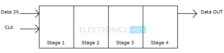
Serial in Serial Out Shift Register
The input to this register is given in serial fashion i.e. one bit after the other through a single data line and the output is also collected serially. The data can be shifted only left or shifted only right. Hence it is called Serial in Serial out shift register or a SISO shift register.
As the data is fed from right as bit by bit, the shift register shifts the data bits to left. A 4-bit SISO shift register consists of 4 flip flops and only three connections.
The registers which will shift the bits to left are called “Shift left registers”.
The registers which will shift the bits to right are called “Shift right registers”.
Example: If we pass the data 1101 to the data input, the shifted output will be 0110.
This one is the simplest register among the four types. As the clock signal is connected to all the 4 flip flops, the serial data is connected to the left most or right most flip flop. The output of the first flip flop is connected to the input of the next flip flop and so on. The final output of the shift register is collected at the outmost flip flop.
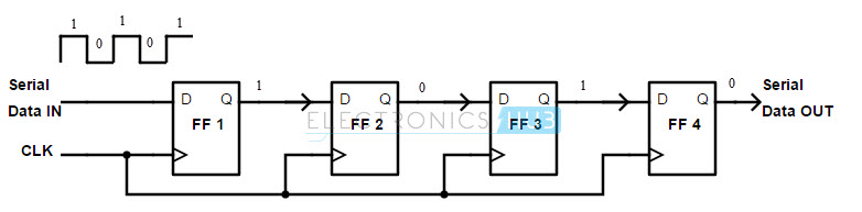
In the above diagram, we see the shift right register; feeding the serial data input from the left side of the flip flop arrangement.
In this shift register, when the clock signal is applied and the serial data is given; only one bit will be available at output at a time in the order of the input data. The use of SISO shift register is to act as temporary data storage device. But the main use of a SISO is to act as a delay element.
Serial in Parallel Out shift register
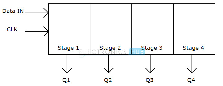
The input to this register is given in serial and the output is collected in parallel
The clear (CLR) signal is connected in addition to clock signal to all the 4 flip flops in order to RESET them and the serial data is connected to the flip flop at either end (depending on shift left register or shift right register). The output of the first flip flop is connected to the input of the next flip flop and so on. All the flip flops are connected with a common clock.
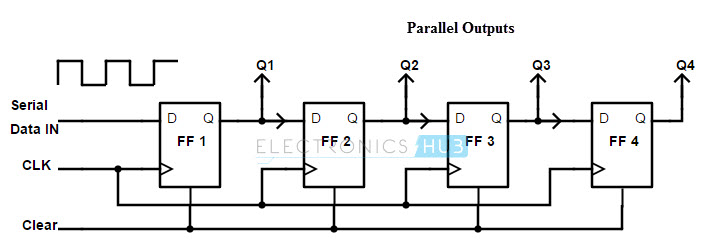
Unlike the serial in serial out shift registers, the output of Serial in Parallel out (SIPO) shift register is collected at each flip flop. Q1, Q2, Q3 and Q4 are the outputs of first, second, third and fourth flip flops, respectively.
The main application of Serial in Parallel out shift register is to convert serial data into parallel data. Hence they are used in communication lines where demultiplexing of a data line into several parallel line is required.
Parallel in Serial out shift register
The input to this register is given in parallel i.e. data is given separately to each flip flop and the output is collected in serial at the output of the end flip flop.
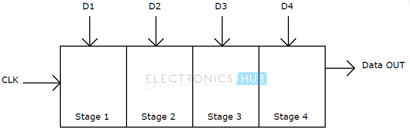
The clock input is directly connected to all the flip flops but the input data is connected individually to each flip flop through a mux (multiplexer) at input of every flip flop. Here D1, D2, D3 and D4 are the individual parallel inputs to the shift register. In this register the output is collected in serial.
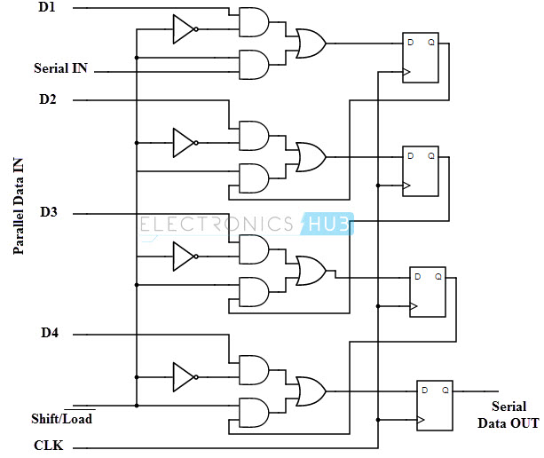
The output of the previous flip flop and parallel data input are connected to the input of the MUX and the output of MUX is connected to the next flip flop. A Parallel in Serial out (PISO) shift register converts parallel data to serial data. Hence they are used in communication lines where a number of data lines are multiplexed into single serial data line.
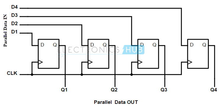
Parallel in Parallel out shift register
In this register, the input is given in parallel and the output also collected in parallel. The clear (CLR) signal and clock signals are connected to all the 4 flip flops. Data is given as input separately for each flip flop and in the same way, output also collected individually from each flip flop.
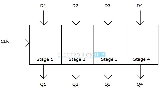
The above diagram shows the 4 stage parallel in parallel out register. Qa, Qb, Qc and Qd are the parallel outputs and Pa, Pb, Pc and Pd are the individual parallel inputs. There are no interconnections between any of the four flip flops.
A Parallel in Parallel out (PIPO) shift register is used as a temporary storage device and also as a delay element similar to a SISO shift register.
Ring Counter
It is designed by connecting the output of the first flip flop to its next one and the output of last flip flop is connected again to the first one as input, like a feedback path. So this is called “Ring Counter”.
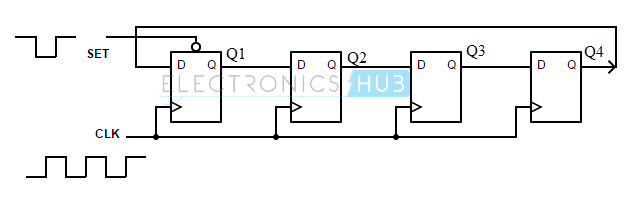
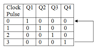
The first flip flop is connected to high input i.e. its input is preset with logic 1 and the output of the first flip flop is connected to input of second flip flop and so on.
Finally, the output of last flip flop is fed back as input to first flip flop. When we apply the first clock pulse to the arrangement; the second stage input changes to 1 and rest inputs are 0. In this way, the input 1 is rotated around the ring.
Other Type of Registers
Apart from the above register types we have the other type of registers also. They are given below.
- Bi directional shift register.
- Universal shift register.
These registers are also used in many applications in digital electronics.
Bidirectional Shift Register
If we shift a binary number to left by one position, this operation is equivalent to multiplying the original number by 2. Similarly, if we shift a binary number to right by one position, this operation is equivalent to dividing the original number by 2.
Hence in order to perform these mathematical operations, we need a shift register that can shift the bits in either direction. This can be achieved by Bidirectional Shift Register.
The entire set of shift registers mentioned above are Unidirectional Shift Registers i.e. they shift the data only to the right or only to the left.
The bidirectional shift register can be defined as “The register in which the data can be shifted either left of right”. This register has mode input for right shift or left shift, a clock signal and two serial Data lines one each for input and output.
The mode input will control the shift left and shift right operations. If the mode input is high (1) then the data will be shifted right. Similarly, if the mode input is low (0) then the data will be shifted left. The circuit of a bidirectional shift register using D flip flops is shown below.
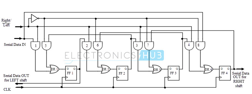
The input serial data is connected at two ends of the circuit (to AND gates 1 and 8). Base on the mode input being high or low, only one AND gate (either 1 or 8) is in active state.
When the mode input is high (Right / Left’ = 1), then the serial data path is
AND1 – OR 1 – FF 1 – Q1 – AND 2 – OR 2 – FF 2 – Q2 – AND 3 – OR 3 – FF 3 – Q3 – AND 4 – OR 4 – FF 4 – Q4 (Serial Data OUT).
When the mode input is low (Right / Left’ = 0), then the serial data path is
AND8 – OR 4 – FF 4 – Q4 – AND 7 – OR 3 – FF 3 – Q3 – AND 6 – OR 2 – FF 2 – Q2 – AND 5 – OR 1 – FF 1 – Q1 (Serial Data OUT).
Universal Shift Register
The universal shift register can be defined as “The register which can be used to shift the data in both the directions like left, right and can load parallel data as well”.
This register can perform three types of operations, stated below.
- Parallel loading
- Shifting left
- Shifting right.
It means that, the universal shift register can store the data in parallel and can transmit the data in parallel. In the same manner the data can stored and transmitted by serial path through shift left and shift right operations.
Simply, the universal shift register will load the data either in serial/parallel and will produce output as we require i.e. either in serial/parallel. It is called Universal Shift Register as it can be used for left shift, right shift, serial to serial, serial to parallel, parallel to serial and parallel to parallel operations.
Construction
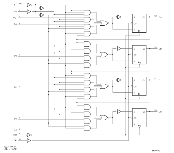
Observe the below logic gate representation of universal shift register. The mode input is directly connected to MUX input and the reversed mode input (using NOT gate) is connected to the inputs of upper stage flip flops.
The inputs D1, D2, D3 and D4 are connected in parallel and the outputs Q1, Q2, Q3 and Q4 are collected in parallel. It has a serial input pin to feed the data into the register for both left shift and right shift. The logic diagram of a 4 bit universal shift register is shown below.
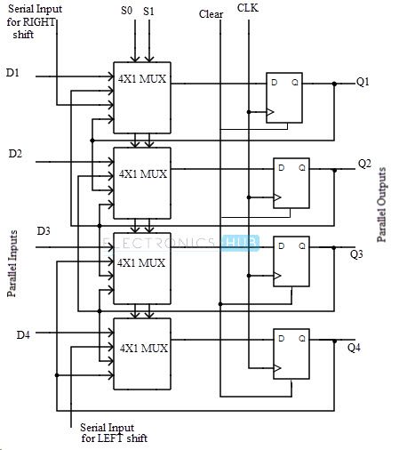
The circuit diagram of a 4 bit bidirectional universal shift register is shown below.
Operation
- The mode input is connected to high (MODE = 1); to load the data in parallel. And for serial shifting, the mode input is connected to low (MODE = 0).
- When the mode pin is connected to GROUND, the universal shift register will operate/ behave as Bi directional shift register.
- To shift the data to right, the input is connected to the AND gate – 1 of the first flip flop; through serial input pin.
- To shift the data to left, the input is connected to AND gate – 8 of the last flip flop; through input D.
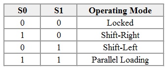
- When S0 = 0 and S1 = 0, then the universal shift register will be in locked state, that means no operation will be performed.
- When S0 = 1 and S1 = 0, then it will shift the data to right, that is shift right operation is performed.
- When S0 = 0 and S1 = 1, then it will shift the data to right, that is shift left operation is performed.
- When S0 = 0 and S1 = 0, then the register results in PARALLEL LOAD operation.
- The universal shift register will operate in all modes shown in above because they have 4×1 MUX at the input.
Applications of Shift Registers
Registers are used in digital electronic devices like computers as
- Temporary data storage
- Data transfer
- Data manipulation
- As counters.
Shift registers are used in computers as memory elements. All the digital systems need to store large amount of data, in an efficient manner; there we use storage elements like RAM and other type of registers.
Many of the digital system operations like division, multiplication are performed by using registers. The data is transferred through serial shift registers and other type.
Counters are used as Digital clocks, Frequency counters, Binary counters etc.
- Serial in – serial out register are used for time delays.
- Serial in – parallel out registers are used for converting the data from serial form to parallel form. So these are also called “Serial to parallel converters”.
- Parallel in – serial out registers are used for converting the data from parallel form to serial form. So these are also called “Parallel to serial converters”.
Delay Line
Introducing Delay line is the most important use of shift registers. A serial in serial out shift register is used to produce time delay, to digital circuits. The time delay can be calculated by using below formula.
Δt = N * 1 / fc
Where N represents number of stages / flip flops and fC represents clock frequency.
So an input pulse is delayed by Δt at output. The amount of time delay is controlled flip flops in the shift register or the clock signal frequency.
Commonly available Shift Register ICs
Generally shift registers are available in 4000 series and 7000 series ICs.
4000 series ICs
- IC 4006 18 stage Shift register.
- IC 4014 8-stage shift register.
- IC 4015 Dual 4-stage shift register.
- IC 4021 8-bit static shift register.
- IC 40104 4 bit bidirectional Parallel-in/Parallel-out PIPO Shift Register.
- IC 40195 4-bit universal shift register.
7000 series ICs
- IC 7491 8-bit shift register, serial in, serial out, gated input.
- IC 7495 4-bit shift register, parallel in, parallel out, serial input.
- IC 7496 5-bit parallel-In/parallel-out shift register, asynchronous preset.
- IC 7499 4-bit bidirectional universal shift register.
- IC 74164 8-bit parallel-out serial shift register with asynchronous.
- IC 74165 8-bit serial shift register, parallel Load, complementary outputs.
- IC 74166 parallel-Load 8-bit shift register.
- IC 74194 4-bit bidirectional universal shift register.
- IC 74198 8-bit bidirectional universal shift register.
- IC 74199 8-bit bidirectional universal shift register with J-Not-K serial inputs.
- IC 74291 4-bit universal shift register, binary up/down counter, synchronous.
- IC 74395 4-bit universal shift register with three-state outputs.
- IC 74498 8-bit bidirectional shift register with parallel inputs and three-state outputs.
- IC 74671 4-bit bidirectional shift register.
- IC 74673 16-bit serial-in serial-out shift register with output storage registers.
- IC 74674 16-bit parallel-in serial-out shift register with three-state outputs.
In these ICs, mostly used are
- 74HC595 Serial-In-Parallel-Out shift register
- 74HC165 Parallel-In-Serial-Out shift register
- 74HC 194 4-bit bidirectional universal shift register
- 74HC 198 8-bit bidirectional universal shift register

4 Responses
finally………understood the whole concept of shift registers!!!!!!!!!
thnku so mch fr this
Now I found, what is a register and it’s types and applications with better understanding, just in couple of minutes.
Thank you ADMINISTRATOR.
Good
Very helpful, easy to understand,, thank you 🙏