In this tutorial, we will try to understand the basics of PNP Tansistor. We ill learn its working, Pins, basic circuit, identification of terminals, example and a few applications.
Introduction
PNP transistor is another type of Bipolar Junction Transistor (BJT). The structure of the PNP transistor is completely different from the NPN transistor. The two PN-junction diodes in the PNP transistor structure are reversed with respect to the NPN transistor, such as the two P-type doped semiconductor materials are separated by a thin layer of N-type doped semiconductor material.
In PNP transistor, the majority current carriers are holes and electrons are the minority current carriers. All the supply voltage polarities applied to the PNP transistor are reversed. In PNP, the current sinks in to the base terminal. The small base current in the PNP has the ability to control the large emitter-collector current because it is a current-controlled device.
The arrow for BJT transistors is always located on the emitter terminal and also it indicates the direction of conventional current flow. In PNP transistor this arrow indicates as ‘pointing in’ and the current direction in PNP is completely opposite to the NPN transistor. The structure of PNP transistor is completely opposite to the NPN transistor. But the characteristics and operation of the PNP transistor is almost same as NPN transistor with small differences. The symbol and structure for PNP transistor is shown below.
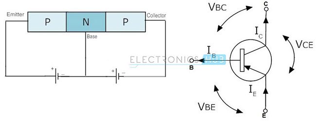
The above figure shows the structure and symbol of PNP Transistor. This transistor mainly consists of 3 terminals and they are Emitter (E), Collector (C) and Base (B). Here if you observe, the base current flows out of the base unlike NPN transistor. The emitter voltage is much positive with respect to base and collector.
PNP Transistor Working
The circuit connection of PNP transistor with supply voltages is given below. Here the base terminal has negative bias with respect to emitter and the emitter terminal has positive bias voltage with respect to both base and collector because of PNP transistor.
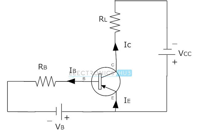
The polarities and current directions are reversed here compared to NPN transistor. If the transistor is connected to all the voltage sources as shown above then the base current flows through the transistor but here the base voltage needs to be more negative with respect to the emitter to operate transistor. Here the base- emitter junction acts as a diode. The small amount of current in the base controls the flowing of large current through emitter to collector region. The base voltage is generally 0.7V for Si and 0.3V for Germanium devices.
Here the base terminal acts as input and the emitter- collector region acts as output. The supply voltage VCC is connected to the emitter terminal and a load resistor (RL) is connected to the collector terminal. This load resistor (RL) is used to limits the maximum current flow through the device. One more resistor (RB) is connected to the base terminal which is used to limit the maximum current flow through the base terminal and also a negative voltage is applied to the base terminal. Here the collector current is always equal to the subtraction of base current from emitter current. Like NPN transistor, the PNP transistor also has the current gain value β. Now let us see the relation between the currents and current gain β.
The collector current (IC) is given by,
IC = IE – IB
The DC current gain (β) for the PNP transistor is same as the NPN transistor.
DC current gain = β = Output current/Input current
Here output current is collector current and input current is base current.
β = IC/IB
From this equation we get,
IB = IC/β
IC = β IB
And also we define the current gain as,
Current gain = Collector current/ Emitter current (In common base transistor)
α = IC/IE
The relation between α and β is given by,
β = α / (1- α) and α = β/ (β+1)
The collector current in PNP transistor is given by,
IC = – α IE + ICBO where ICBO is the saturation current.
Since IE = -(IC + IB)
IC = – α (-(IC + IB)) + ICBO
IC – α IC = α IB + ICBO
IC (1- α) = α IB + ICBO
IC = (α/ (1- α)) IB + ICBO/ (1- α)
Since β = α / (1- α)
Now we get the equation for collector current
IC = β IB + (1+ β) ICBO
The output characteristics of PNP transistor are same as NPN transistor characteristics. The small difference is that the PNP transistor characteristic curve rotates 1800 to calculate the reverse polarity voltages and current values. The dynamic load line also exists on the characteristic curve to calculate the Q-point value. The PNP transistors are also used in switching and amplifying circuits like NPN transistors.
PNP Transistor Example
Consider a PNP transistor, which is connected in the circuit with the supply voltages VB = 1.5V, VE = 2V, +VCC = 10V and –VCC = -10V. And also this circuit connected with the resistors of RB = 200kΩ and RE = RC (or RL) = 5kΩ. Now calculate the current gain values (α, β) of the PNP transistor.
Here
VB = 1.5V
VE = 2V
+VCC = 10V and –VCC = -10V
RB = 200kΩ
RE = RC (or RL) = 5kΩ
Base current,
IB = VB/ RB = 1.5/ (200*103) = 7.5uA.
Emitter current,
IE = VE/ RE = (10-2)/ (5*103) = 8/ (5*103) = 1.6mA.
Collector current,
IC = IE – IB = 1.6*10-3 – 7.5*10-6 = 1.59mA.
Now we have to calculate α and β values,
α = IC/IE = 1.59*10-3/1.6*10-3 = 0.995
β = IC/IB = 1.59*10-3/7.5*10-6 = 212
Finally we get the current gain values of a considered PNP transistor are,
α = 0.995 and β = 212
BJT Transistor Matching
Transistor matching is nothing but connecting the both NPN and PNP transistors in a single design to generate high power. This structure is also called as “matched pair”. The both NPN and PNP transistors are called complementary transistors. Mainly these matched pair circuits are used in power amplifiers, such as class B amplifiers. If we connect the complementary transistors which are having the same characteristics then it is very useful to operate the output stages in motors and large machinery designs by producing high power continuously.
The NPN transistor conducts only in the positive half cycle of signal and the PNP transistor conducts only in the negative half cycle of the signal, due to this the device operates continuously. This continuous operation is very useful in the power motors to produce continuous power. The complementary transistors need to have same DC current gain (β) value. These matched pair circuits are used in motors controlling, robotics and power amplifier applications.
PNP Transistor Identification
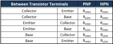
Generally we identify the PNP transistors with their structure. We have some differences in the structures of both NPN and PNP transistors when compared. One more thing to identify the PNP transistor is generally the PNP transistor is in OFF for positive voltage and it is in ON when small output current and negative voltage at its base with respect to emitter. But to identify them with most efficiently we use some other technique by calculating the resistance between the three terminals, such as base, emitter and collector.
We have some standard resistance values for identifying the both NPN and PNP transistors. It is necessary to test each pair of terminals in both directions for resistance values so totally six tests are needed. This process is very much useful to identify the PNP transistor easily. Now we see the operation behavior of each pair of terminals.
- Emitter-Base Terminals: The emitter-base region acts as a diode but it conducts only in one direction.
- Collector-Base Terminals: The collector-base region also acts as diode which conducts I only one direction.
- Emitter-Collector Terminals: The emitter- collector region looks like a diode but it will not conduct in either direction.
Now let us see the resistance value table to identify both NPN and PNP transistors as shown in the following table.
PNP Transistor as a Switch
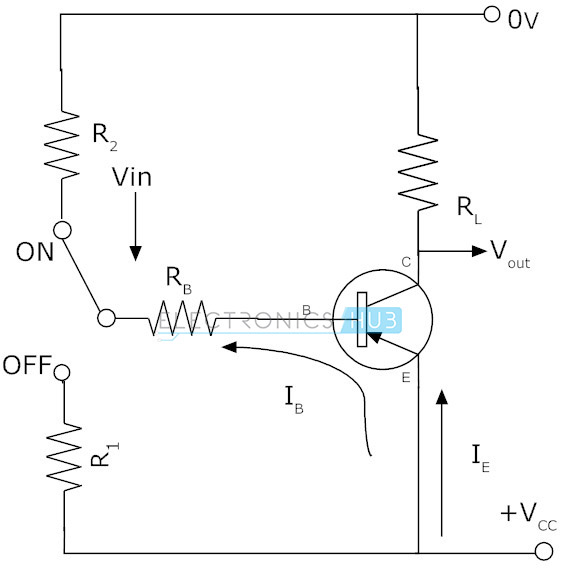
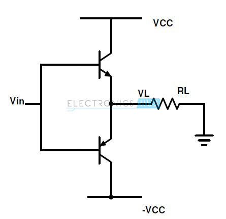
The circuit in the above figure shows the PNP transistor as a switch. The operation of this circuit is very simple, if the input pin of transistor (base) is connected to ground (i.e. negative voltage) then the PNP transistor is in ‘ON’, now the supply voltage at emitter conducts and the output pin pulled up to the larger voltage. If the input pin connected to the high voltage (i.e. positive voltage) then the transistor is ‘OFF’, so the output voltage has to be low (zero). This operation shows the switching conditions of a PNP transistor due to their ON and OFF states.
Applications
- PNP transistors are used to source current, i.e. current flows out of the collector.
- PNP transistors are used as switches.
- These are used in the amplifying circuits.
- PNP transistors are used when we need to turnoff something by push a button. i.e. emergency shutdown.
- Used in Darlington pair circuits.
- Used in matched pair circuits to produce continuous power.
- Used in heavy motors to control current flow.
- Used in robotic applications.

12 Responses
thanxx for this but i need working of pnp and npn configuration.
Nice
Very effective for me thou…
Not that bad…
Very useful tutorial about transistor which i got on this website.
Excellent.
good identification of PNP transistor
never could figure out PNP Transistor but this brush up read I got a better understanding of its operation thanks
Hello, Riga: the collector current is given by: Ic = -aIb + Ic (sat). Why Ic (sat)? – Next line:
Ie = – (Ic + Ib) why less? which becomes (next line) (-Ic + Ib)? Further on. PNP example. Row: base current:
Ib = Vb / Rb and Vce? Then Emitter current: Ie = Ve / Re = (10-2) / Re and Rc (Rl). Clarifications I need to reinforce the few certainties I have as a neophyte. Thank you
The site is very effective on research and am satisfied
One of my lecturer copy and paste this tutorial for us as a course
Very usefulll now bcz there are my jee exams ahead thankyou …….
Good explaination and example thanks.
Thank I have got useful information for my assignment