In this tutorial, I’ll show you the steps for How to Design PCB using Eagle CAD Software. After designing the PCB in Autodesk’s Eagle CAD, I’ll show you to make your own PCB (Printed Circuit Board) at home.
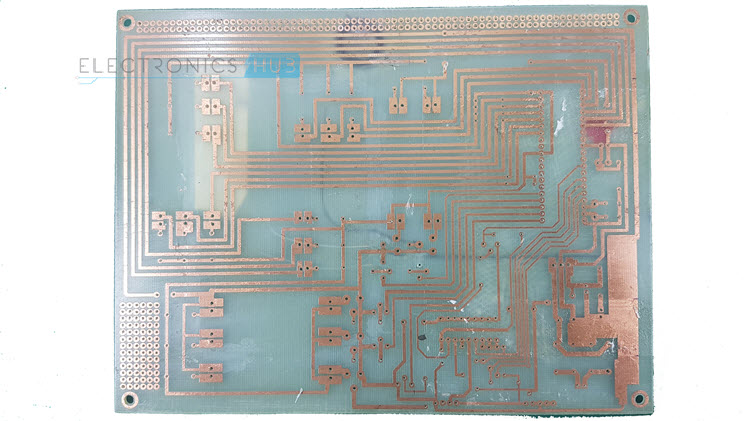
A PCB or Printed Circuit Board is a board that contains several electrical components that are connected using conductive electrical tracks. A PCB provides physical support for mounting the electronic components and also the electrical connections between them.
Students, hobbyists and beginners in electronics often start working on electronic circuits using breadboards. They are suitable for small projects which involve a limited number of components (through-hole components) and connections.
Why do we need PCBs?
If you want to make your design more appealing, then PCBs are the next step. With the help of PCBs, we can avoid common problems like noise, distortion, imperfect contact, etc. Moreover, if you want to go commercial with your design, you have to use a proper circuit board.
But, many people, especially beginners, will find it difficult to design circuit boards as they feel it as a tedious job and requires extreme knowledge in circuit board design. Designing printed circuit boards is actually simple (yes, it does need some practice and efforts).
Also read this post: A list of PCB Design Softwares
How to Design a PCB Layout Using Eagle
Step for making your own PCB
In this article, I’ll show you a step-by-step tutorial on how to design PCB using Eagle and also make your own PCB at home. For this you will need to follow the three steps or procedures:
- Designing schematic of the design
- Drawing the layout for the Printed Circuit Board (PCB) and
- Making the board (there are different ways to do this)
The first two tasks i.e. schematic and circuit board layout are done with the help of a CAD Tool. There are many CAD Tools for designing PCBs like Altium Designer, Cadence OrCAD, Mentor Graphics PADS, Autodesk Eagle, KiCad, etc.
In this tutorial, we are going to use Autodesk Eagle CAD. Eagle is available in three variants: Eagle Free, Eagle Standard and Eagle Premium.
Eagle Free, as the name suggests, is a free to use PCB design software which can be used for capturing schematics and PCB Layout. The other two variants are subscription based software and have additional features like more schematic sheets, more signal layers and more board area.
You can download the free version of the Eagle PCB from the Autodesk’s official website or follow this link. https://www.autodesk.com/products/eagle/free-download
How to Design PCB using Eagle CAD?
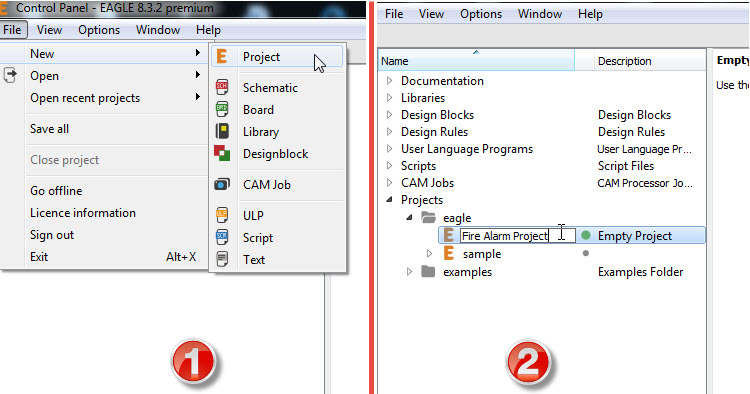
After downloading and installing the Eagle CAD (you might need to register with Autodesk), open the Eagle Software from the desktop shortcut. You will get the control Panel of the Eagle.

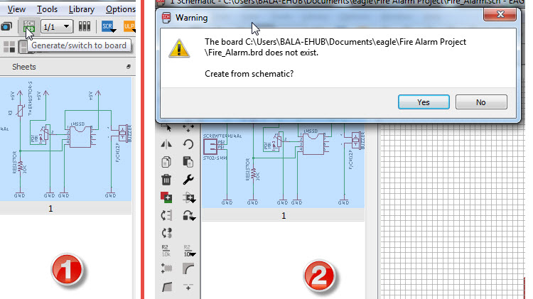
Click on File and select New Project. Rename the Project to an appropriate name (I will be designing the PCB for Fire Alarm Project). Right click on the project and create new schematic.
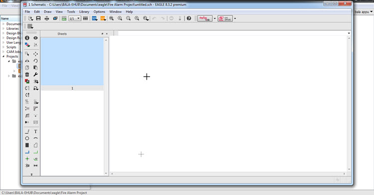
Designing Schematic for PCB
A new schematic window will open with a blank work space. This is called the Schematic Editor, where you can draw schematics of your design. Save the schematic file with extension .sch.
After this, we have to add the necessary components which we are going to use in our schematic. But, before that, we need to adjust the grid size of the schematic. Select the Grid option and set the size to 1mm. Also set the alternate grid to a smaller value. You can turn on the grid by selecting display on option.
NOTE: Setting Grid is optional and set the values you are comfortable with.
Now, we have to add components to our schematic. For this, select Add Option from the side tool bar. A new window opens with a list of all the components available in the libraries.

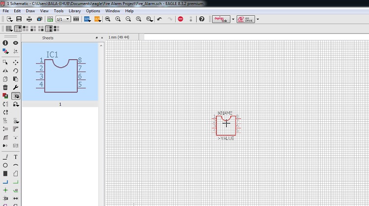
The first component is the Op – Amp, which is an 8 – pin DIP. So, instead of adding the IC directly, we will add an 8 – pin DIP Socket. So, go to the library ic-package and select DIL8 component. Alternatively, you can use the search option at the bottom, if you know the name of the component.
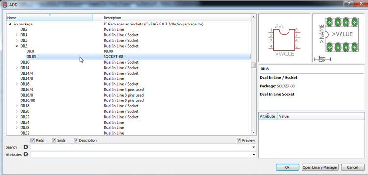
After selecting the component, in our case an 8 – pin DIP Socket, click on OK and then you can place the component on the schematic sheet. Click on the sheet once to place the component and if you want to rotate the component, right click. After placing the component on the schematic, press Esc to return to the component selection window.
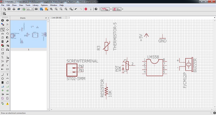
Similarly, add the rest of the components required to complete the circuit. The components are: a square type POT, quarter watt resistor, small buzzer, a thermistor and a two pin screw terminal. Additionally, add the +5V and GND symbols from the supply library.
After placing all the components, rename the components to something understandable. Also, mention the values like 10KΩ Resistor etc.
Connecting Components in Schematic
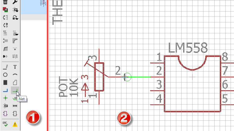
Next step is to connect these components. You have to use the net option from the side tool bar and start making the connections.
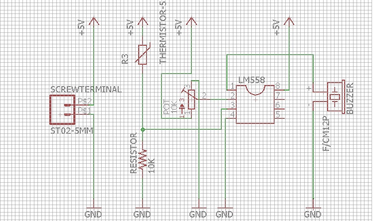
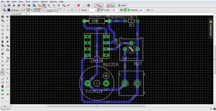
After making all the connections, the final schematic will look something like the circuit in the following image. Save the schematic file.
PCB Layout Design
After completing the schematic, we have to proceed with the design of the PCB layout. Select the switch to board option from the top tool bar. You can create the board fie from the schematic.
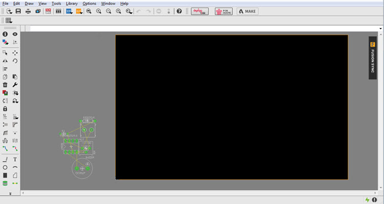
A new window opens which is the PCB layout editor. The black space is the board area and all the components are at the outside bottom left of the board area. Now, we need to place the components in to the editor. You can adjust the grid size of the PCB Layout editor, if you want.
Now, using the group option from the side tool bar, select all the components and using move option move all the components and populate the board area.
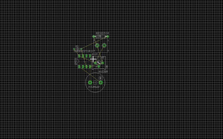
Using the move option, place the components on the board as per the position you want the component to be on the board. You can see thin yellow wires running between the components. These wires are called air wires and are representation of connections between components.
When we route the path between components, these air wires will disappear as an indication of successful connection.
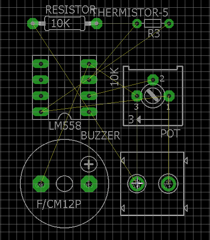
Now, it is time to make the connections or traces for the Printed Circuit Board. For this, we are going to use the Route tool from the side tool bar. Also set the width of the trace to be routed as your requirement. Here, I’ve set the trace width to approximately 1mm. Then, select the signal layer i.e. bottom layer, as our PCB is a single sided board.
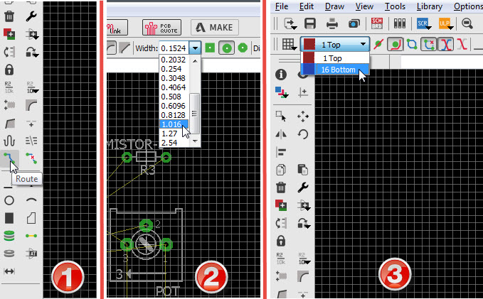
Start routing the traces from pin to pin. As you progress with routing, the air wires will start disappearing.

Complete all the connections and make sure that one trace do not interact with other (as this is considered as a short circuit).
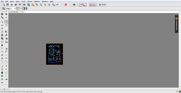
Adjust the size of the board as per the required dimensions and save the file. The board file will be save with .brd extension. Before proceeding with how to make your own PCB at home, I’ll show you one more important step: the Ground Pour.
Select the polygon option from the side tool bar and start drawing the polygon along the edges of the board. Make sure that the signal layer is bottom. The starting and ending points of the polygon must meet.
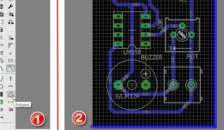
You will get a dotted line along the edges of the board. Select name option and rename the polygon to GND. Hit ratsnest option from the side tool bar to see the ground pour.
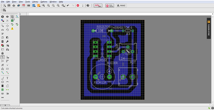
The layout for the PCB is ready. The next step is to check for errors and generate the necessary gerber files for sending them to PCB Manufacturers.
Also read this article on HOW TO DESIGN PCB USING KiCAD?
In this article, I’ve shown you how to get started with Eagle and basics of PCB Design using Eagle CAD. But here we only finished the design part. In the next tutorial, I’ll show you how to use this PCB Layout from Eagle CAD and make your own PCB at home.

One Response
Basically, PCBs are used to prevent problems such as noise, distortion, imperfect contact, and other problems with commercial designs as you’ve mentioned. That is quite an interesting thing to learn as it would be very helpful for those in the technology field as it would make things way smoother with their equipment’s functionality. I’ll try reading more about these PCBs and how I can make use of them if need be. Thanks!