In this tutorial, we will learn about different Applications of Operational Amplifiers. Op-Amps are one of the basic analog circuits that have a wide range of implementations. We will learn some of the important but more commonly used Operational Amplifier Application in this post.
Op-amp Comparator
A comparator, in electronics, is a circuit configuration that compares two voltages (or currents) and indicates which one is larger. Thus, the inputs to a comparator should be different in nature. Comparators can be easily configured using op-amps, since the op-amps have high gain and balanced difference inputs.
Theoretically, an op-amp in open-loop configuration (no feedback) can be used as a comparator. When the input voltage at the non-inverting terminal V+ is greater than the voltage at the inverting input terminal V–, the output of the op-amp saturates at its positive extreme. When the non-inverting input voltage drops below the inverting input voltage, the op-amp output switches to its negative saturation level. Comparator circuits are most widely used in analog-to-digital converters (ADCs) and in oscillators.
Op-amp Inverting Comparator
In an inverting comparator, the input voltage Vin is applied to the inverting input terminal of the op-amp and the non-inverting input terminal is connected to reference voltage, through resistors R1 and R2. As long as the input voltage Vin is lesser than the reference voltage Vref, the output of the op-amp remains positively saturated. When Vin goes above the reference voltage, the output of the op-amp switches to its negative saturation level and remains negatively saturated as long as Vin is less than Vref. The circuit of a comparator using op-amp is shown in the figure below.
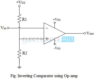
By choosing the values of resistors R1 and R2, the reference voltage Vref can be adjusted and comparator can be used to compare input voltage with the corresponding reference voltage.
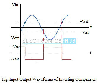
Vout = +Vsat; if Vin < Vref
= -Vsat; if Vin > Vref
The input and output waveforms of an op-amp inverting comparator is shown in the figure below.
Op-amp Non-Inverting Comparator
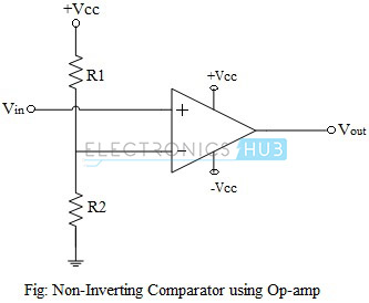
In the case of an op-amp non-inverting comparator, the input voltage Vin is applied to the non-inverting input terminal and the reference voltage, Vref, is connected to the inverting input terminal. When the input voltage Vin is greater than the reference voltage Vref, the op-amp output is positively saturated. In practice, the difference (Vin-Vref) will be a positive value. Since there is no feedback to the op-amp input, the open-loop gain of the op-amp will be infinity. Hence the output will swing to its maximum possible value, +Vsat. When the input voltage falls below the reference voltage, the output switches to its negative saturation voltage.
Vout = +Vsat ; if Vin > Vref
= -Vsat ; if Vin < Vref
Op-amp Logarithmic Amplifier
An operational amplifier can be configured to function as a Logarithmic amplifier, or simply Log amplifier. Log amplifier is a non-linear circuit configuration, where the output is K times the logarithmic value of the input voltage applied. Log amplifiers find the applications in computations such as multiplication and division of signals, computation of powers and roots, signal compression and decompression, as well as in process control in industrial applications. A log amplifier can be constructed using a bipolar junction transistor in the feedback to the op-amp, since the collector current of a BJT is logarithmically related to its base-emitter voltage.
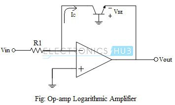
The circuit of a fundamental log amplifier using op-amp is shown in the figure above. The necessary condition of the log amplifier to work is that the input voltage always must be positive. It can be seen that Vout = – Vbe.
Since the collector terminal of the transistor is held at virtual ground and the base terminal is also grounded, the voltage-current relationship becomes that of a diode and is given by,
IE = IS.[eq(Vbe)/kT – 1]
Where,
IS = the saturation current,
k = Boltzmann’s constant
T = absolute temperature (in K)
Since IE = IC for grounded base transistor,
IC = IS. [eq(Vbe)/kT – 1]
(IC/IS) = [eq(Vbe)/kT – 1]
(IC/IS) + 1 = [eq(Vbe)/kT]
(IC+IS)/IS = eq(Vbe)/kT
eq(Vbe)/kT = (IC/IS) since IC >> IS
Taking natural log on both sides of the above equation, we get
Vbe = (kT/q) ln[IC/IS]
The collector current IC = Vin/R1 and Vout = -Vbe
Therefore,
Vout = -(kT/q) ln[Vin/R1.IS]
The output of the circuit is, thus, proportional to the log of the input voltage. However, the output is dependent on the saturation current which varies from transistor to transistor and also with temperature. Compensation circuits can be added to stabilize the output against these variations.
Anti-Logarithmic Amplifier or Exponential Amplifier
Anti-logarithmic or exponential amplifier (or simply antilog amplifier) is an op-amp circuit configuration, whose output is proportional to the exponential value or anti-log value of the input. Antilog amplifier does the exact opposite of a log amplifier. Antilog amplifiers along with log amplifiers are used to perform analogue computations on the input signals. The circuit of an antilog amplifier using op-amp is shown in the figure below.
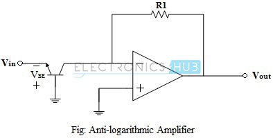
It is noted that by exchanging the positions of the transistor and the resistor, the log amplifier can be made to work as antilog amplifier. The base-collector voltage of the transistor is maintained at ground potential, from the virtual ground concept. The current IE for the transistor is given by,
IE = IS.[eq(Vbe)/kT – 1]
For a grounded base transistor, IE = IC. Therefore,
IC = IS.[eq(Vbe)/kT – 1]
Where, IS = saturation current of the transistor,
Vout = IC.R1
Vout = IS.[eq(Vbe)/kT – 1].R1
Also, for the above circuit Vin = -Vbe. Therefore,
Vout = R1.IS.[eq(-Vin)/kT – 1]
Antilog amplifiers also suffer from unstable outputs, due to the variations in IS for different transistors and temperature dependence. Compensating circuits can be added to stabilize the output against such variations.
Current to Voltage Converter
An operational amplifier current-to-voltage converter, also known as a Trans-Impedance amplifier, is a circuit which converts the change in the input current to a corresponding output voltage. The current to voltage converter circuit is most commonly used to amplify the current output of photodiodes, photo-detectors, accelerometers and other sensor devices to a noticeable and usable voltage level.
A simple current-to-voltage converter circuit will have a feedback resistor, with a large value of resistance. The gain of the amplifier is dependent on this resistor. Depending on the application, a current-to-voltage converter can be constructed in different ways. All the configurations convert the low-level current output of a sensor device to a significant voltage level. The gain and the bandwidth of the circuit changes with different types of sensors.
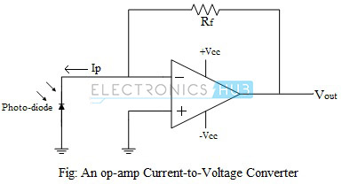
The circuit of a basic current-to-voltage converter is shown in the figure above. The sensor device, in this case is a photo-diode, and it is connected to the inverting input terminal and the non-inverting input terminal is grounded. This provides a low impedance load for the photo-diode, which keeps the voltage across the photo-diode low. The high gain of the op-amp keeps the photo-diode current, Ip, equal to the feedback current through resistor Rf. The input offset voltage due to the photo-diode is very low, since the photo-diode has no external bias. This provides a large output gain, without any output offset voltage.
The output voltage of the above circuit can be given as,
Vout = – IP.Rf
The above equation satisfies only for the DC and low-frequency gain current-to-voltage converter. If the gain is large, any input offset voltage at the non-inverting input of the op-amp will result in an output offset voltage. To minimize these effects, the current-to-voltage converters are usually designed with FETs at the op-amp input, which have very low input offset voltages.
Op-amp Inverter
An op-amp inverting amplifier, or inverter, inverts the input signal as well as amplifies it. A positive-going signal at the input of an inverting amplifier would result in a negative-going signal at the output and vice versa .An AC sinusoidal signal at the input would produce 180o out of phase sinusoidal signal at the output.
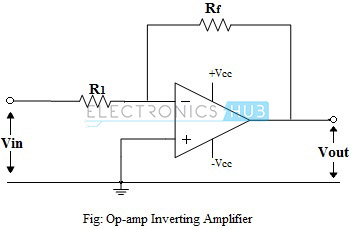
Above figure shows the circuit of a typical inverting amplifier using an op-amp. The circuit uses a negative feedback connection, through the resistor Rf. The input signal is applied to the inverting input terminal and the non-inverting input terminal is grounded.
Since the input current to the op-amp is ideally zero, the current I due to the input voltage flows through resistors R1 and Rf. The input and output voltages can be calculated as,
Vin = I.R1
Vout = -I.Rf
Therefore, the closed-loop gain of the circuit, ACL, is
ACL = Vout/Vin = – (I.Rf/I.R1) = -Rf/R1
The input voltage Vin is thus amplified by -Rf/R1 times at the output. It can be noted that if the resistances of both the resistors, R1 and Rf, are equal then the output voltage is,
Vout = – Vin
Such a circuit is known as an inverting buffer, or simply an Inverter.
Op-amp Non-Inverting Amplifier
A non-inverting amplifier is an op-amp circuit configuration which produces an amplified output signal that is in-phase with the input signal applied. A non-inverting amplifier uses a negative feedback connection, but instead of feeding the entire output signal to the input, only a part of the output signal voltage is fed back as input to the inverting input terminal of the op-amp.
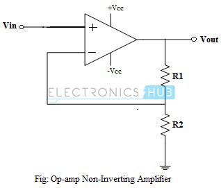
Above figure shows a typical non-inverting amplifier. The input signal is applied to the non-inverting input terminal and the output is fed to the inverting input terminal through a resistive potential divider network.
When a positive-going input signal is applied to the non-inverting input terminal, the output voltage will shift to keep the inverting input terminal equal to that of the input voltage applied. Hence, there will be a feedback voltage developed across resistor R2,
VR2 = VIN = I2R2
Where, I2 is the current flowing at the junction of resistors R1 and R2.
VOUT = I2 (R1 + R2)
From the above equations of VIN and VOUT, the closed-loop voltage gain of the non-inverting amplifier can be calculated as,
ACL = VOUT/VIN
= I2 (R1 + R2) / I2R2
= (R1 + R2) / R2
ACL = 1 + (R1/R2)
The above gain equation is positive, indicating that the output will be in-phase with the applied input signal. The closed-loop voltage gain of a non-inverting amplifier is determined by the ratio of the resistors R1 and R2 used in the circuit.
Practical non-inverting amplifiers will have a resistor in series with the input voltage source, to keep the input current equal in both input terminals.
Op-amp Applications Summary
This article presents an overview of the wide range of applications of an operational amplifier. An op-amp can be used to perform various mathematical operations such as addition, subtraction, multiplication along with calculus operations like differentiation and integration. Op-amps are used for a variety of applications such as AC and DC signal amplification, filters, oscillators, voltage regulators, comparators in most of the consumer and industrial devices. Today, op-amps are very popular building blocks in analogue electronic circuits.
