NPN transistor is one of the Bipolar Junction Transistor (BJT) types. The NPN transistor consists of two n-type semiconductor materials and they are separated by a thin layer of p-type semiconductor. Here the majority charge carriers are the electrons. The flowing of these electrons from emitter to collector forms the current flow in the transistor. Generally the NPN transistor is the most used type of bipolar transistors because the mobility of electrons is higher than the mobility of holes. The NPN transistor has three terminals – emitter, base and collector. The NPN transistor is mostly used for amplifying and switching the signals.
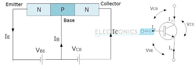
The above figure shows the symbol and structure of NPN transistor. In this structure we can observe the three terminals of transistor, circuit currents and voltage value representations. Now let us see the operation of the NPN transistor with explanation.
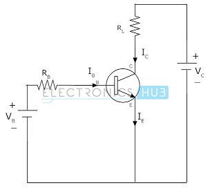
Bipolar NPN Transistor Circuit
The above figure shows the NPN transistor circuit with supply voltages and resistive loads. Here the collector terminal always connected to the positive voltage, the emitter terminal connected to the negative supply and the base terminal controls the ON/OFF states of transistor depending on the voltage applied to it.
Operation Of NPN Transistor
The working of NPN transistor is quite complex. In the above circuit connections we observed that the supply voltage VB is applied to the base terminal through the load RB. The collector terminal connected to the voltage VCC through the load RL. Here both the loads RB and RL can limit the current flow through the corresponding terminals. Here the base terminal and collector terminals always contain positive voltages with respect to emitter terminal.
If the base voltage is equal to the emitter voltage then the transistor is in OFF state. If the base voltage increases over emitter voltage then the transistor becomes more switched until it is in fully ON state. If the sufficient positive voltage is applied to the base terminal i.e. fully-ON state, then electrons flow generated and the current (IC) flows from emitter to the collector. Here the base terminal acts as input and the collector-emitter region acts as output.
To allow current flow between emitter and collector properly, it is necessary that the collector voltage must be positive and also greater than the emitter voltage of transistor. Some amount of voltage drop presented between base and emitter, such as 0.7V. So the base voltage must be greater than the voltage drop 0.7V otherwise the transistor will not operate. The equation for base current of a bipolar NPN transistor is given by,
IB = (VB-VBE)/RB
Where,
IB = Base current
VB = Base bias voltage
VBE = Input Base-emitter voltage = 0.7V
RB = Base resistance
The output collector current in common emitter NPN transistor can be calculated by applying Kirchhoff’s Voltage Law (KVL).
The equation for collector supply voltage is given as
VCC = ICRL + VCE ………… (1)
From the above equation the collector current for common emitter NPN transistor is given as
IC = (VCC-VCE)/RL
In a common emitter NPN transistor the relation between collector current and emitter current is given as
IC = β IB
In active region the NPN transistor acts as a good amplifier. In common emitter NPN transistor total current flow through the transistor is defined as the ratio of collector current to the base current IC/IB. This ratio is also called as “DC current gain” and it doesn’t have any units. This ratio is generally represented with β and the maximum value of β is about 200. In common base NPN transistor the total current gain is expressed with the ratio of collector current to emitter current IC/IE. This ratio is represented with α and this value is generally equal to unity.
α, β and γ Relationship in NPN Transistor
Now let us see the relationship between the two ratio parameters α and β.
α = DC current gain for common base circuit = Output current/Input current
In common base NPN transistor output current is collector current (IC) and input current is emitter current (IE).
α = IC/IE ………..(2)
This current gain (α) value is very close to unity but less than the unity.
We know that the emitter current is the sum of small base current and large collector current.
IE = IC + IB
IB = IE – IC
from equation 2, the collector
IC = αIE
IB = IE – αIE
IB = IE (1-α)
β = DC current gain for common emitter circuit = Output current/Input current
Here output current is collector current and input current is base current.
β = IC/IB
β = IC/IE (1-α)
β = α/(1-α)
From the above equations the relationship between α and β can be expressed as
α = β (1-α) = β/(β+1)
β = α (1+β) = α/ (1-α)
The β value may vary from 20 to 1000 for low power transistors which operate with high frequencies. But in general this β value can have the values in between the range of 50-200.
Now we will see the relationship between α, β and γ factors.
In common collector NPN transistor the current gain is defined as the ratio emitter current IE to base current IB. This current gain is represented with γ.
γ = IE/IB
We know that emitter current
IE = IC + IB
γ = (IC + IB )/IB
γ = (IC/IB) + 1
γ = β +1
Hence the relationships between α, β and γ are given as below
α = β / (β+1), β = α / (1-α), γ = β +1
NPN Transistor Examples
1. Calculate the base current IB to switch a resistive load of 4mA of a Bipolar NPN transistor which having the current gain (β) value 100.
IB = IC/β = (4*10-3)/100 =40uA
2. Calculate the base current of a bipolar NPN transistor having the bias voltage 10V and the input base resistance of 200kΩ.
We know the equation for base current IB is,
IB = (VB-VBE)/RB
We know the values,
VBE = 0.7V,
VB = 10V,
RB = 200Ω.
Now we substitute these values in the above equation,
We get,
IB = (VB-VBE)/RB= (10-0.7)/200kΩ = 46.5uA.
The base current of NPN transistor is 46.5uA.
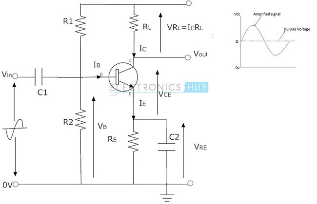
Common Emitter Configuration
The common emitter configuration circuit is one of the three BJT configurations. These common emitter configuration circuits are used as voltage amplifiers. Generally the BJT transistors have three terminals but in the circuit connections we need to take any one terminal as common. So we use one of the three terminals as common terminal for both input and output actions. In this configuration we use emitter terminal as common terminal, thus it is named as common-emitter configuration.
This configuration is used as a single stage common emitter amplifier circuit. In this configuration base acts as input terminal, collector acts as output terminal and emitter as common terminal. The operation of this circuit starts with biasing the base terminal such that forward biasing the base-emitter junction. The small current in the base controls the current flow in the transistor. This configuration always operates in the linear region to amplify the signals at output side.
This common emitter amplifier gives the inverted output and can have very high gain. This gain value is influenced by temperature and bias current. The common-emitter amplifier circuit is mostly used configuration than other BJT configurations because of its high input impedance and low output impedance and also this configuration amplifier provides high voltage gain and power gain.
The current gain for this configuration is always greater than unity usually the typical value is about 50. These configuration amplifiers are mostly used in the applications where low frequency amplifier and radio frequency circuits are required. The circuit diagram for the common-emitter amplifier configuration is shown below.
Output Characteristics of NPN Transistor
The family of output characteristics curves of a bipolar transistor is given below. The curves show the relationship between the collector current (IC) and the collector-emitter voltage (VCE) with the varying of base current (IB). We know that the transistor is ‘ON’ only when at least a small amount of current and small amount of voltage is applied at its base terminal relative to emitter otherwise the transistor is in ‘OFF’ state.
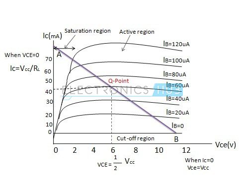
The collector current (IC) is mostly affected by the collector voltage (VCE) at 1.0V level but this IC value is not highly affected above this value. Already we know that the emitter current is the sum of base and collector currents. i.e. IE =IC+ IB. The current flowing through the resistive load (RL) is equal to the collector current of the transistor. The equation for the collector current is given by,
IC= (VCC-VCE)/ RL
The straight line indicates the ‘Dynamic load line’ which is connecting the points A (where VCE = 0) and B (where IC = 0). The region along this load line represents the ‘active region’ of the transistor.
The common emitter configuration characteristics curves are used to calculate the collector current when the collector voltage and base current is given. The load line (red line) is used to determine the Q-point in the graph. The slope of the load line is equal to the reciprocal of the load resistance. i.e. -1/RL.
Input Characteristics of NPN Transistor
Unlike the output characteristics, which focus on the collector current, the input characteristics explore the relationship between the transistor’s base current (IB) and the base-emitter voltage (VBE). Here, the key aspect is how changes in VBE affect IB, highlighting the transistor’s sensitivity to input signals applied at the base.
Input characteristics are typically presented for the transistor’s active region. This showcases how a small change in VBE can lead to a significant increase in IB, forming the basis for current amplification in transistors.
Understanding input characteristics is crucial for anyone working with transistors, especially in the common-emitter configuration. Here, the input characteristics directly influence the overall circuit performance.
NPN Transistor Applications
- NPN transistors are mainly used in switching applications.
- Used in amplifying circuit applications.
- Used in the Darlington pair circuits to amplify weak signals.
- NPN transistors are used in the applications where there is a need to sink a current.
- Used in some classic amplifier circuits, such as ‘push-pull’ amplifier circuits.
- In temperature sensors.
- Very High frequency applications.
- Used in logarithmic convertors.

6 Responses
we are also interested is topic of very useful for students
Excellent support and issue project s !!
Good support for students
This is the best article to show the relationship between Schottky characteristic curves and the output characteristics curves of a bipolar NPN transistor.
At my age of 82 years I am benefitted by the article.Thanks. Let your service grow for people of my age too;
Abraham Joseph, M.Sc., M.Phil.
Male:Associated Professor of Chemistry, Retired./
age 82 years running.
Thank u very much for giving such knowledge .But,I want more information about it’s practical.
This is really really very useful for me… Thank you for these ❤️ information 😊