Detection of light is a basic need for everything like plants, animals and even devices. Device researchers have worked on techniques for light detection and developed devices that offer excellent performance. Light is an electromagnetic radiation with a much shorter wavelength and higher frequency than radio waves. It is a quantum mechanical phenomena and comes in discrete particles called Photons.
What Is Light Sensor?
A light sensor is a passive sensor that is used to indicate the intensity of the light by examining the radiant energy that exists in a certain range of frequencies. In the spectrum of electromagnetic waves, the ranges of frequencies that are used to detect using a sensor are between infrared to visible and up to ultraviolet.
Light sensors convert the light energy in the form of photons to electrical energy in the form of electrons. Hence, they are also called as Photo Sensors or Photo Detectors or Photo Electric Devices.
Light sensors or Photo Sensors can be classed into three types based on the physical quantity that is affected. The main classes are Photo resistors, photo voltaic and photo emitters. Photo emitters generate electricity when exposed to light. Photo resistors change their electrical properties when illuminated. Based on the above classes, the following classification of devices can be made.
Photo Emissive Cells: These types of photo devices release free electrons from light sensitive materials when strike by a photon of sufficient energy. The generally used light sensitive material is Caesium. The energy of a photon is dependent on the wavelength or frequency of the light.
The equation of energy of a photon is
E = hc / λ
Here,
h is Planck’s constant (h = 6.626 * 10-34 J s),
c is velocity of light (c = 3 * 108 m / s)
λ is wavelength of the light.
If the frequency of the light is higher, the energy of the photon is higher.
Photo Conductive Cells: These types of photo devices vary their electrical property of resistance when they are subjected to light. The common type of photoconductive material is Cadmium Sulphide (CdS) which is used in Light Dependent Resistor Photocells. The photoconductivity in these cells results from light hitting a semiconductor material which controls the flow of current through it. For a given applied voltage, when the intensity of the light increases, the current also increases.
Photo Voltaic Cells: These types of photo devices generate a potential or an emf that is proportional to the energy of the radiant light. Solar Cells are a common type of photo voltaic cells and use Selenium as the photo voltaic material. They are made by sandwiching two semiconductor materials and when light energy is incident on them, a voltage of approximately 0.5 V is generated.
Photo Junction Diodes: These types of photo devices are generally semiconductor devices and use light to control the flow of electrons or holes across the junctions. Photo Diodes and Photo Transistors are the two main devices in this category. They are specifically designed for detector applications.
Light Dependent Resistor (LDR)
When subjected to light energy, a Photoconductive light sensor will change its physical property. Photo Resistor is a common type of photoconductive device. Photo resistor is a semiconductor device that uses light energy to control the flow of electrons and therefore the flow of current in them.
The most common type of photoconductive cell is a Light Dependent Resistor or LDR. As the name implies, a Light Dependent Resistor is a semiconductor device that changes its electrical resistance depending on the presence of light. A Light Dependent Resistor changes its electrical resistance from a high value of several thousand Ohms in the dark to only a few hundreds of Ohms when light is incident on it by creating electron – hole pairs in the material.
The most common material used to make a Light Dependent Resistor is Cadmium Sulphide (CdS). Other materials like Lead Sulphide (PbS), Indium Antimonide (InSb) or Lead Selenide (PbSe) can also be used as the semiconductor substrate.
Cadmium Sulphide is used in Photo resistors that are sensitive to near infrared and visible light. The reason it is used is because of its close resemblance of its spectral response curve to that of the human eye. It can be controlled by a simple, light source like a flash light and the peak sensitive wavelength of Cadmium Sulphide material is about 560 nm to 600 nm in the visible spectral range.
Cadmium Sulphide is deposited as a thread pattern on an insulator in the shape of a zigzag line as shown below.
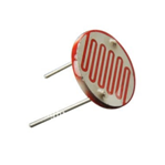
The reason for zigzag path is to increase dark resistance and therefore decrease the dark current. This cell is encapsulated in a glass to protect the substrate from contamination.
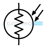
The symbol of photo resistor is shown below.
The most popular type of photoconductive cell is ORP12 Cadmium Sulphide photo conductive cell.
The characteristics of ORP12 type of photo conductor cell are as follows: the peak spectral response is 610 nm, dark resistance is 10 MΩ and resistance when illuminated is 100 Ω.
Light Dependent Resistor Voltage Divider Network
A Light Dependent Resistor is generally connected in series with a resistor with a single DC voltage supply across it. The connection is shown below.
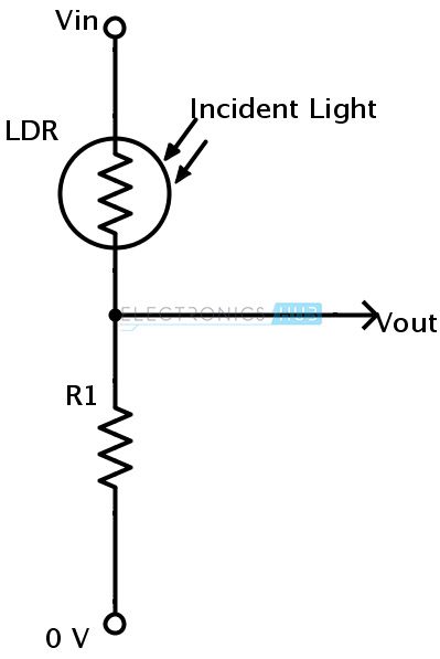
The advantage of this connection is the appearance of different voltages at their junction for different intensities of light. This connection is an example of a Voltage Divider Network or Potential Divider. The reason is because the resistive value of the light dependent resistor RLDR will determine the amount of voltage drop across the series resistor R1.
The current in a series connection is same and as the resistance of the light dependent resistor changes due to the light intensity, the output voltage will be determined by using the voltage divider formula.
The output voltage VOUT = VIN * (R1 / (RLDR + R1 )).
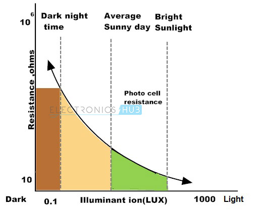
In the absence of light, the resistance of a light dependent resistor is as high as 10 M Ω. In the presence of sunlight, the resistance of a light dependent resistor will fall to 100 Ω. The variation of the resistance of a light dependent resistor over different intensities of light is shown in the below curve.
Light Sensitive Switch is a common application of Light Dependent Resistor. The circuit of a Light Dependent Resistor Switch is shown below.
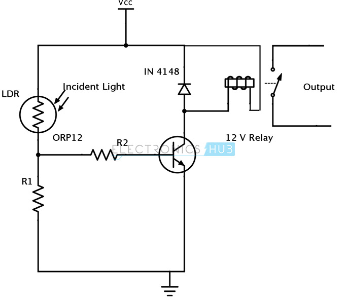
It is a light sensor circuit with relay output light activated switch. The Light Dependent Resistor RLDR and the resistor R1 form a voltage divider network. When there is no light, i.e. in darkness, the resistance of Light Dependent Resistor is in the order of mega Ohms. The base bias voltage is zero and the transistor is OFF.
As the intensity of the light increases, the resistance of the Light Dependent Resistor decreases and the bias voltage increases. At a certain point determined by the voltage divider network, the bias voltage raises enough to turn the transistor ON. This in turn activates the relay which can be used to control some other external circuit.
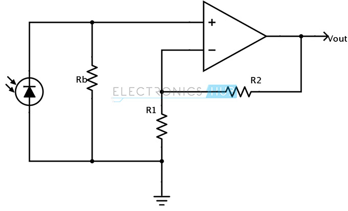
Light Sensing Circuit Using LDR
The sensitivity of the LDR switch is fairly low. To increase the sensitivity of light sensing, few modifications can be applied. The fixed resistor R1 is replaced with a potentiometer VR1. The transistor is replaced with an Operational Amplifier and the light dependent resistor is incorporated into a Wheatstone bridge. The new and more sensitive light sensing circuit using a light dependent resistor is shown below.
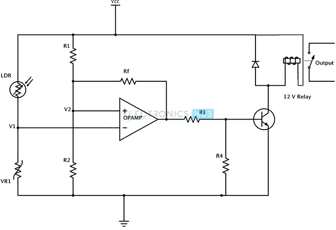
The resistors LDR, VR1, R1 and R2 will form a Wheatstone bridge. The sides of bridge LDR – VR1 and R1¬ – R2 form a potential divider with output voltages V1 and V2. These voltages are connected to non-inverting and inverting inputs of the operational amplifier respectively. The operational amplifier is operated as a differential amplifier whose output is a function of the difference between the two input voltages V1 and V2. This is also known as a voltage comparator with feedback. The feedback resistor Rf is used to provide required voltage gain.
The output of the operational amplifier is connected to a relay which can control an external circuit. When the voltage V1 due to light sensing by LDR falls below the voltage V2, which acts as a reference voltage, the output of the amplifier changes its state. This causes the relay to activate and the load is switched on.
As the intensity of the light increases, the output switches back and the relay is turned off.
Here the relay is turned on when the intensity of light is less. The operation can be reversed by reversing the positions of the light detecting resistor and potentiometer. Now the relay is turned on when the light level increases and exceeds the level set by the reference voltage.
Photodiode
Photodiode is in the class of photo junction device which is basically a PN junction light sensor. They are generally made from semiconductor PN junctions and are sensitive to visible light and infrared light. When light is incident on a Photodiode, the electrons and holes are separated and will allow the junction to conduct.
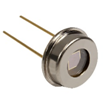
Photodiodes are constructed like any other conventional junction diodes. A typical photo diode is shown below.
The opaque coating used in signal and rectifier diodes is absent in photo diodes. This makes the diode transparent enough to permit light and to affect the conductivity of the junction.
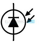
The symbol of a photo diode is shown below.
Principle of Operation
A photo diode is biased against its easy flow of direction of current, i.e. it is reverse biased so that a very low leakage current flows. If a photon of sufficient energy is incident on the diode at its junction, an electron is freed and if it possesses enough energy, it may pass over the energy barrier causing a small leakage current to flow. The amount of current is proportional to the amount of illumination of the junction.
Photo Diode Characteristics
In the absence of light, the current – voltage characteristic of a photo diode is similar to that of a normal diode. Similar to a normal diode, there is an exponential increase in current when a photo diode is forward biased. When it is reverse biased, a small leakage current called reverse saturation current will appear and causes an increase in the depletion region.
When a photo diode is used as a light sensor, for Germanium type diodes, the dark current is around 10 µA and for Silicon type diodes, it is 1 µA. Dark current is the current when the intensity of the light is 0 Lux.
Light Sensing using Photodiode
Photodiode may be operated and biased in two modes: photo voltaic mode and photoconductive mode.
In photo voltaic mode, the photo diode is connected to a virtual ground preamplifier. The circuit is shown below.
When photons incident, a voltage is generated and is amplified by the operational amplifier. Apart from the thermally generated current, there is no basic leakage current as there is no DC bias across the diode.
A similar circuit which converts the current generated by the light to voltage and amplified by an op amp is shown below.

These circuits utilize the characteristic of the op amp in which the two input terminals are at zero voltage to operate the diode without any DC bias. This configuration of the op amp gives a high impedance load to the photo diode resulting in a wider range of current relative to the intensity of incident light.
In photoconductive mode, the photodiode is DC biased, and the current flowing across the diode is due to DC bias as well as light sensing is converted to voltage by the resistor and is amplified by the operational amplifier. This approach widens the depletion region as the applied bias decreases the capacitance of the photo diode.
The circuit of photodiode in photoconductive mode is shown below.
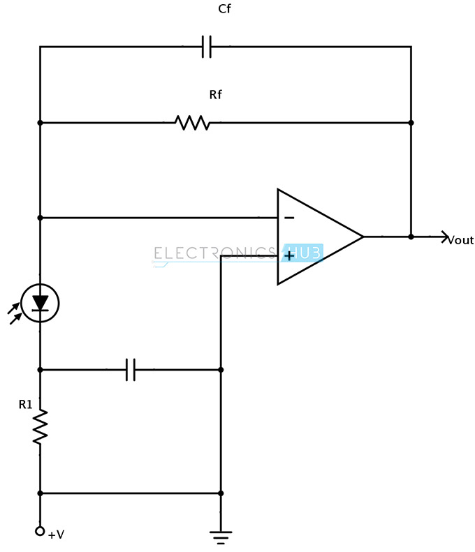
The capacitor is used to set the output bandwidth as 1 / (2πRFCF) and also prevents oscillations. However, there is a delay of RC as the capacitor must charge.
Phototransistor
In addition to making photo junction devices from diodes, it is possible to construct a light sensor from transistors. Figuratively, a photo transistor is basically a combination of a photo diode and an amplification transistor.
The representation of a phototransistor with photodiode and a transistor is shown below.
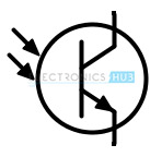
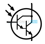
The symbol of photo transistor is shown below.
In a photo transistor, the collector – base junction acts as a photo diode. The collector – base junction is reverse biased exposing it to a light source. The current at this junction is amplified by normal transistor action and hence the collector current is large.
Principle of Operation
The operation of a phototransistor is similar to that of a photodiode. The additional benefits are they can provide large collector current and sensitive than photodiodes. The currents in a photo transistor are 50 to 100 times greater than that in case of a photodiode. By connecting a photodiode between the collector and base terminals of a normal transistor, it can be converted to a photo transistor.
Photo Transistor Characteristics
Photo transistors are basically NPN transistors with their large base terminal electrically isolated or unconnected. To control the sensitivity, some photo transistors allows base connection. If a base connection is used, a base current is generated when the photons hit the surface, and causes a collector to emitter current to flow.
In order to achieve reverse bias at collector – base junction, the collector is at a higher potential with respect to the emitter. In the absence of light, a small amount of normal leakage current flows. In the presence of light on base terminal, the number of electron – hole pairs in this region increases and current produced is amplified by the transistor operation.
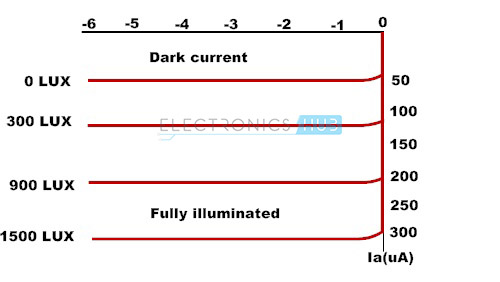
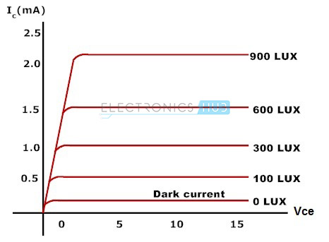
The relationship between light intensity, current and output voltage is shown below.
Light Sensing Using Photo Transistor
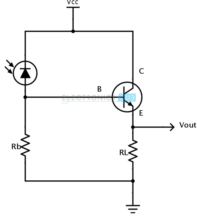
A simple circuit used to sense light which involves a photo transistor is shown below.
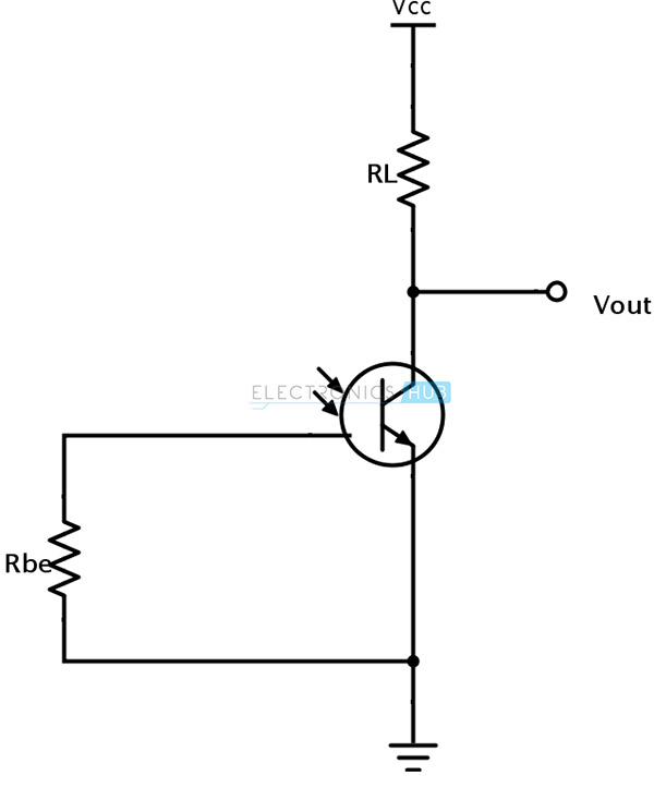
The sensitivity of a photo transistor is dependent on the DC current gain of the transistor. Hence, the overall sensitivity, which is a function of collector current, can be controlled by the resistance between emitter and base.
For high sensitivity applications, like Optocouplers, a Darlington Photo Transistor is used. It is generally called a Photo Darlington Transistor and uses a second bipolar NPN junction transistor. This second transistor will provide additional amplification.
The circuit of a photo transistor with second transistor is shown below.
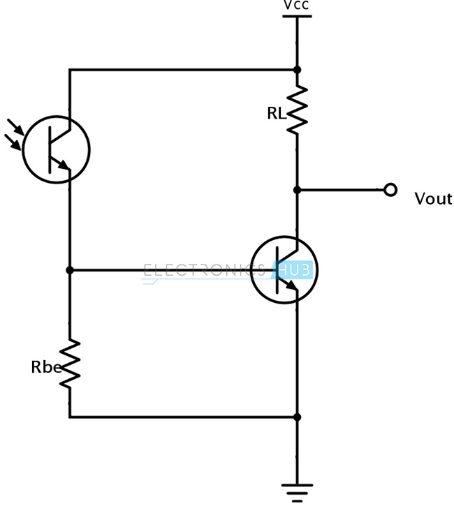
The symbol of a Photo Darlington Transistor is shown below.
A Photo Darlington Transistor consists of a photo transistor whose emitter output is coupled to the base terminal of a second larger NPN transistor. A photo Darlington device is a very sensitive detector as the total current gain is the product of individual current gains.

3 Responses
Please share photo transistor based dusk to down switch in more details
Very easy to follow. Thank you.
I haave metalshield photo cell has no 41 on side it came from footpedal volume control on kawai organ I need a replacement wire leads have been broken off can idetify or tell me size ot type.