Latch is an electronic logic circuit with two stable states i.e. it is a bistable multivibrator. Latch has a feedback path to retain the information. Hence a latch can be a memory device. Latch can store one bit of information as long as the device is powered on. When enable is asserted, latch immediately changes the stored information when the input is changed i.e. they are level triggered devices. It continuously samples the inputs when the enable signal is on.
Latch circuits can work in two states depending on the triggering signal being high or low: Active – High or Active – Low.
- In case of Active – High latch circuits, normally both the inputs are low. The circuit is triggered by a momentary high on either of the inputs.
- In case of Active – Low latch circuits, normally both the inputs are high. The circuit is triggered by a momentary low on either of the inputs.
SR LATCH
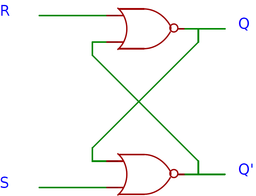
We can use static gates as basic building blocks in order to construct a simple latch and it can be constructed with two NOR gates by introducing feedback to a NOR gate circuit.
A simple NOR gate logic with feedback is shown below.
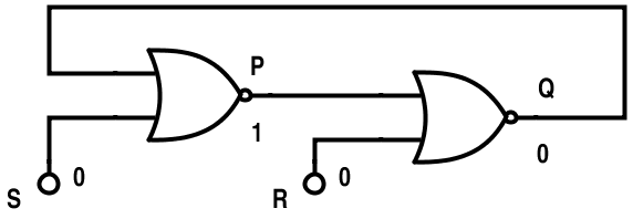
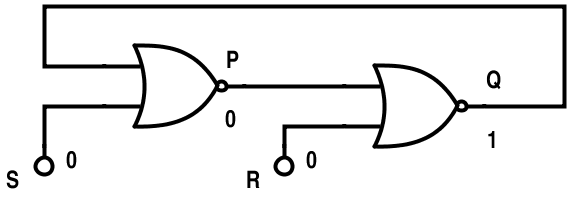
Here, both the inputs S and R are 0 (S = R = 0). The output of first NOR gate is P = 1. This is fed to the second NOR gate along with R = 0. Hence the output of the second gate is Q = 0. The circuit is said to be in stable state with P = 1 and Q = 0. If we make S = 1, then P = 0. This will make Q =1 as shown below.

This is also a stable state. If S is made 0, there is no change as Q = 1 is fed back to first NOR and P still remains 0. It is shown in the below figure.
If R is made 1, then Q becomes 0 which will change P back to 1.

If R is made 0, then there is no change and we arrive at where we started.
As the output depends not only on present inputs but also on past sequence of inputs, the circuit is said to have memory. If the input condition S = R = 1 is not allowed, the stable state outputs are always complementary. When both S and R are equal to 1, P = 0 and Q = 0 which contradicts the complementary condition. Hence the input condition S = R = 1 is said to be not allowed. The latch circuit is always drawn as a cross coupled form to emphasize the symmetry between the gates.
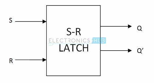
In this circuit, when S = 1, it ‘sets’ the output Q to 1 and when the input R = 1, it ‘resets’ the output Q to 0. With the restriction of S = R = 1, this circuit is called a Set – Reset Latch (SR Latch).
RACE AROUND CONDITION
In logic circuits, Race condition means “The situation at which the two inputs of a logic circuit change at the same time and that will make the output tentative”. The inputs are in competition to change the output. It generally happens in the devices which have the output as the feed-back input of the circuit. It is an unwanted situation that occurs when a device attempts to perform two operations at the same time (i.e. changing the state of two inputs simultaneously). There are few ways in which we can avoid race around condition like using Edge Triggering or by using Master Slave Flip – flop.
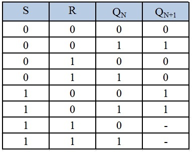
State Transition Table or Truth Table of SR Latch
State table is similar to truth table in combinational circuits that gives the information about the states of a circuit. As the outputs of sequential circuits depend on present and previous states, these are represented in the form of table called state table and it shows the next state based on the present state and other inputs.
The state table for SR latch is shown below.
State Diagram
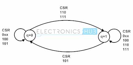
In addition to tables and equations, a state machine (or a system) can be represented by a state diagram. In this state diagram, a state is represented by a circle, and the transition between states is represented by lines or arcs that connect the circles. State diagram for a simple SR latch is shown below.
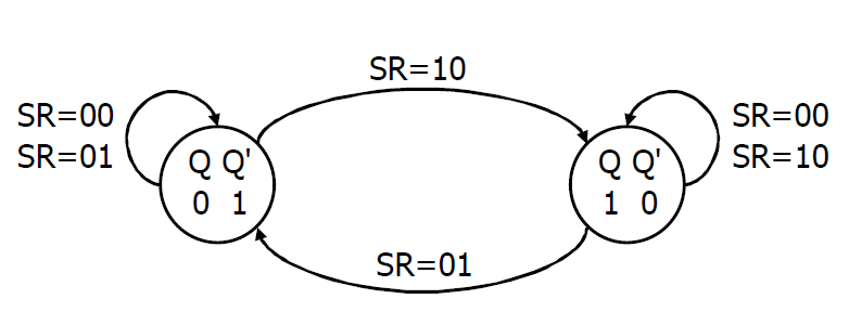
The state diagram provides all the information that a state table can have. This is obtained from the state table directly.
GATED S-R LATCH
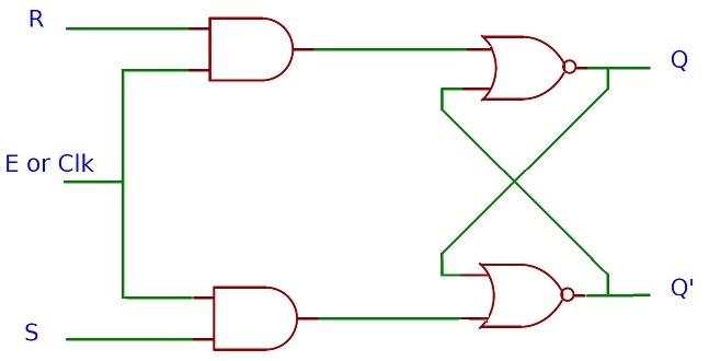
Generally, latches are transparent i.e. the output changes immediately when there is a change in the input. But for many applications, it is desirable to have an isolated period where the output doesn’t change even when there is a change in the input. During this period, the outputs are said to be truly ‘latched’. This can be achieved with the use of an extra input (enable or clock or gate). If the enable (or clock or gate) signal is not asserted, the inputs are ignored and the outputs are latched to the previous values. In order to use this extra signal, additional logic should be added. These circuits are called Gated or Clocked Latches.
Gated SR latch can be made in two ways: by adding second level of AND gates to SR latch or by adding second level of NAND gates to ̅S ̅R latch (Inverted SR latch).
The circuit diagram of Gated SR latch constructed from NOR gates is shown below.
The circuit diagram of Gated SR latch constructed from NAND gates is shown below.
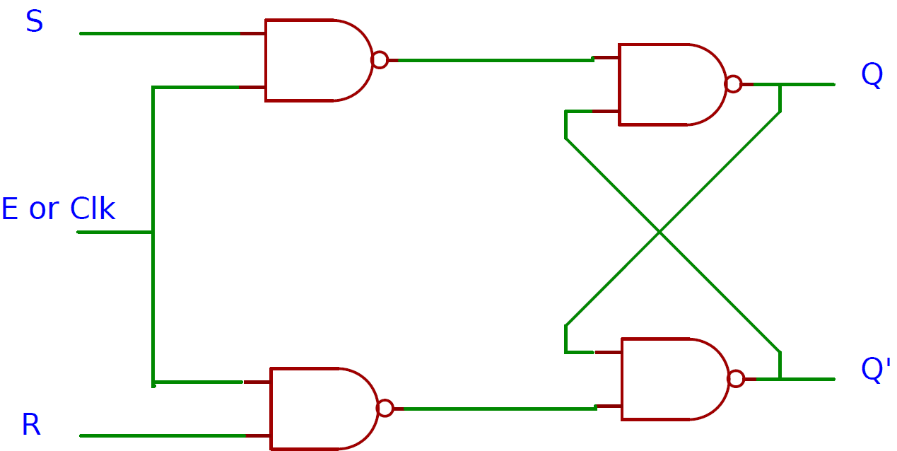
As the NAND gate inverts the inputs, ̅S ̅R latch becomes a gated SR latch.
When enable (or clock) is high, the latch is said to be enabled i.e. the output responds to the inputs.
When enable (or clock) is low, the latch is disabled and remains in that state until enable is asserted.
The symbol for gated SR latch is shown below

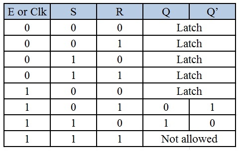
The truth table for gated SR latch is tabulated below.
The state diagram of gated SR latch is shown below.
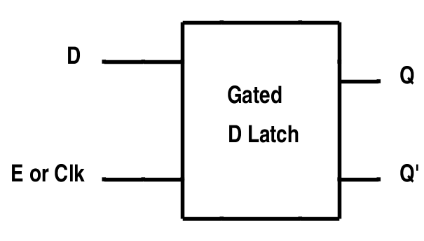
D Latch
Data latch or Delay latch (D latch) is one of the simple latches to store data. It is also called transparent latch. A simple D latch can be constructed with two NAND gates.
The race around condition in SR latch that occurs when S = R = 1 can be avoided in D latch as the R input is replaced with inverted S which is renamed to D. hence there are no illegal or forbidden inputs. In a D latch, Q always D.
The symbol for D latch is shown below.

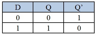
These simple D latches are not frequently used but Gated D latches are very common. The truth table of a simple D Latch is shown below.
GATED D LATCH
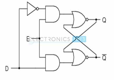
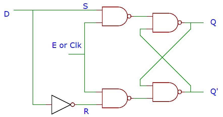
A gated D latch can be easily constructed by modifying a gated SR latch. The only modification to the gated SR latch is that the R input has to be changed to inverted S. A gated latch formed from NOR SR latch is shown below.
When the clock or enable is high (logic 1), the output latches whatever is on the D input. When the enable or clock is low (logic0), the D input for the last enable high will be the output.
This latch circuit will never experience a “Race” condition because the single D input is inverted to provide to both the inputs. Hence, there is no chance for same input condition. So the D latch circuit can be safely used in any circuit.
The symbol of gated D latch is shown below.
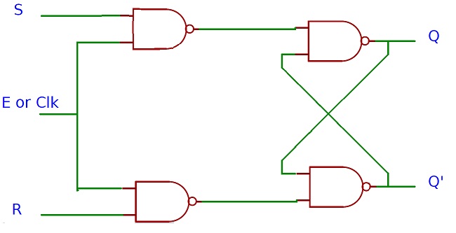
Similar to gated NOR SR latch, a gated D latch can also be constructed from gated NAND SR latch. The circuit for gated D latch from gated NAND SR larch is shown below.
The usage of inverter can be avoided as the NAND gate can be used to obtain the inverted value. Some modification is required in the above circuit and the resultant circuit is shown below.
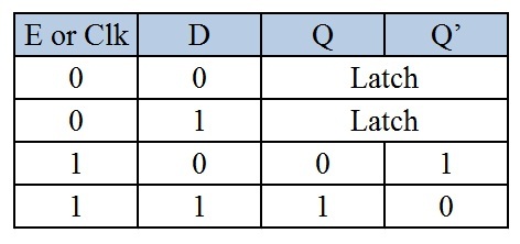
The truth table (or state table) of a gated D latch is shown below.
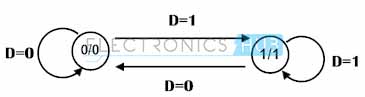
The state diagram of s gated D latch is shown below.
 Latches Applications
- They are basic 1 – bit memory devices.
- D latches are typically used as I/O ports in asynchronous systems.
- Data latches are sometimes used in synchronous two phase systems to reduce the transistor count.
Advantages of latches
- Latch is faster because it has no need to wait for a clock signal so they are most used in high speed designs.
- They require less power.
- Latch based designs have small die-size.
- The major advantage of the latches is “Time-Borrowing”. In which if an operation is not completed within time, the required time for executing the operation is borrowed from the other operational time.
Disadvantages of latches
- Latch less predictable because there is more chance to affect to race conditions.
- Level sensitive devices and hence more chance of metastability.
- Analysing of Latch circuits is difficult because of its level sensitive property.

One Response
THIS IS A MARVELOUS WORK. AM SO MUCH GRATEFUL .