In this tutorial, we will learn about a variation of Field Effect Transistors (FET) called Junction Field Effect Transistor or simply JFET. We will see the circuit symbols, basic biasing condition, the V-I characteristics, a simple amplifier circuit and few applications.
Introduction
The FET transistors are voltage controlled devices, where as the BJT transistors are current controlled devices. The FET transistors have basically three terminals, such as Drain (D), Source (S) and Gate (G) which are equivalent to the collector, emitter and base terminals in the corresponding BJT transistor.
In BJT transistors the output current is controlled by the input current which is applied to the base, but in the FET transistors the output current is controlled by the input voltage applied to the gate terminal.
In the FET transistors the output current passes between the drain and source terminals and this path is called channel and this channel may be made of either P-type or N-type semiconductor materials. In BJT transistor a small input current operates the large load, but in FET a small input voltage operates the large load at the output.
The BJT transistors are ‘bipolar’ devices because they operates with both types of charge carriers, such as electrons and holes but the FET transistors are ‘unipolar’ devices because they operate with the charge carriers of either electrons (for N-channel) or holes (for P-channel).
The FET transistors can be made smaller in size compared to BJT transistor and also they have less power dissipation. Due to this high efficiency the FET transistors are used in many electronic circuit applications by replacing the corresponding BJT transistors. These FET transistors are very useful in the chip designing due to their low power consumption behavior. Like BJT the FET transistors are also available in both P-channel and N-channel.
The FET transistors have high input impedance where as BJT has relatively low. Due to this high impedance values the FET transistors are very sensitive to small input voltages. The FET transistors are mainly classified into two types; they are Junction Field Effect Transistor (JFET) and Insulated Gate FET (IG-FET) or Metal Oxide Semiconductor FET (MOSFET).
Junction Field Effect Transistor (JFET)
The Junction Field Effect transistor (JFET) is one of the types of FET transistors. JFET is a simplest form of FET transistors and it has three terminals. The JFET transistors are used as electronically controlled switches, Voltage controlled resistors and as amplifiers.
BJT transistors are constructed with the PN-junctions but the JFET transistors have a channel instead of the PN-junctions. This channel is formed due to the either of P-type or N-type semiconductor materials.
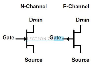
The JFET transistors are classified into two types; they are N-channel JFET and P-channel JFET. In the N-channel JFET the channel is doped with the donor impurities due to this the current passing through the channel is negative (i.e. due to electrons) but in the P-channel JFETs the channel is doped with the acceptor impurities due to this the current flowing through this channel is positive (i.e. due to holes).
The N-channel JFET has more current conduction than P-channel JFET because the mobility of electrons is greater than the mobility of holes. So the N-channel JFETs are widely used than P-channel JFETs. The small voltage at the gate (G) terminal controls the current flow in the channel (between drain and source) of the JFET.
The emitter and collector terminals are connected using PN-junctions in BJT but in JFET the Drain and Source terminals are connected with the channel. The small voltage applied at the gate terminal controls the current flow in the channel between the drain and source of the JFET. This gate voltage is negative in N-channel JFET and it is positive in P-channel JFET.
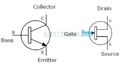
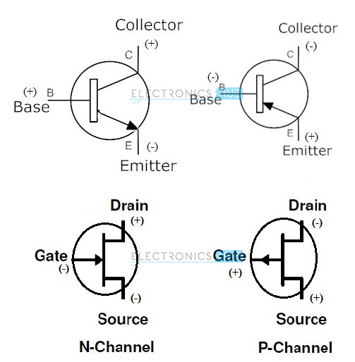
One of the main differences between the BJT and JFET transistors is that when the JFET has reverse-biased junction, then the gate current may be zero, but in the BJT the base current always must be greater than zero. The comparison of symbols between BJT and JFET is shown in the below figures.
N-channel JFET Biasing
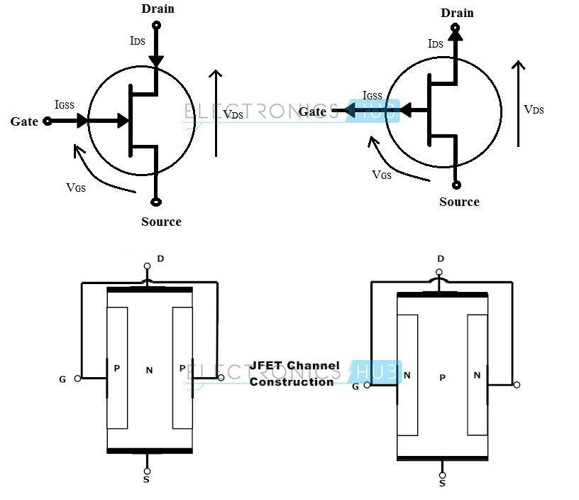
The internal diagram for N-channel JFET transistor is shown below. This is a transistor with N-type of channel and with P-type materials of the region. If the gate is diffused into the N-type channel, then a reverse biased PN-junction is formed which results a depletion region around the gate terminal when no external supply is applied to the transistor. Generally the JFETs are called as depletion mode devices.
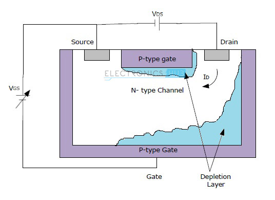
This depletion region produces a potential gradient with the variation of thickness around the PN-junction. This PN-junction opposes the current flow through the channel by reducing the channel width and by increasing the channel resistance.
Now the channel of JFET conducts with zero bias voltage applied as input. Because of the large portion of the depletion region formed between the gate-drain and the small portion of the depletion region between gate and source.
If small voltage (VDS) applied between the drain-source with zero gate voltage (VG) then current (IDS) will flow through this channel. Now if we apply a small amount of negative voltage (-VGS) (i.e. reverse biased condition) then the depletion region width increases, which results in decreasing the portion of the channel length and reduces the conduction of the channel.
This process is called “squeezing effect”. If we will increase more negative voltage at the gate terminal then it reduces the channel width until no current flows through the channel. Now at this condition the JFET is said to be “pinched-off”. The applied voltage at which the channel of FET closes is called as “pinched-off voltage (VP)”.
Pinch-off Effect
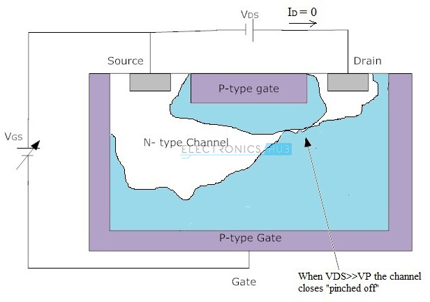
The JFET with N-channel structure is shown above. At primarily if the gate voltage is zero, then the channel resistance is also zero and the conduction of the channel is high. If the gate voltage (i.e. negative voltage) increases to above zero, then the resistance of the channel also increases and the small amount of current will flows through the channel.
If we apply a large amount of negative voltage at the gate terminal, then the channel totally blocks the flow of current through it. In this condition, there is no current flow through the channel and now the JFET acts as a perfect resistor.
The state of JFET in which the channel closes is called “pinched-off” and the voltage applied at gate in that situation is called “pinched-off voltage (VP)”. At the pinched-off condition the gate voltage (VGS) controls the channel current. The P-channel JFET operation is same as the N-channel JFET with some variations, such as the channel current is positive because of the conduction due to holes and it is needed the reverse polarity to apply gate voltage.
JFET V-I Characteristics
The V-I characteristics of N-channel JFET are shown below. In this N-channel JFET structure the gate voltage (VGS) controls the current flow between the source drain. The JFET is a voltage controlled device so no current flows through the gate, then the source current (IS) is equal to the drain current (ID) i.e. ID = IS.
In this V-I characteristic the voltage VGS represents the voltage applied between the gate and the source and the voltage VDS represents the voltage applied between the drain and source.
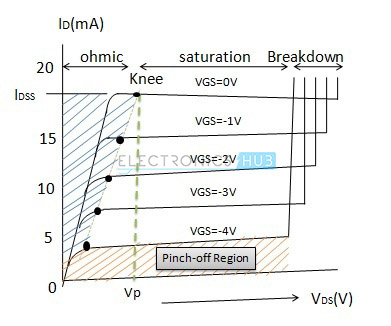
The JFET has different characteristics at different stages of operation depending on the input voltages and the characteristics of JFET at different regions are explained below. Mainly the JFET operates in ohmic, saturation, cut-off and break-down regions.
Ohmic Region: If VGS = 0 then the depletion region of the channel is very small and in this region the JFET acts as a voltage controlled resistor.
Pinched-off Region: This is also called as cut-off region. The JFET enters into this region when the gate voltage is large negative, then the channel closes i.e.no current flows through the channel.
Saturation or Active Region: In this region the channel acts as a good conductor which is controlled by the gate voltage (VGS).
Breakdown Region: If the drain to source voltage (VDS) is high enough, then the channel of the JFET breaks down and in this region uncontrolled maximum current passes through the device.
The V-I characteristic curves of P-channel JFET transistor are also same as the N-channel JFET with some exceptions, such as if the gate to source voltage (VGS) increases positively then the drain current decreases.
The drain current ID flowing through the channel is zero when applied voltage VGS is equal to pinch-off voltage VP. In normal operation of JFET the applied gate voltage VGS is in between 0 and VP, In this case the drain current ID flowing through the channel can be calculated as follows.
ID = IDSS (1-(VGS/VP))2
Where
ID = Drain current
IDSS = maximum saturation current
VGS = gate to source voltage
VP = pinched-off voltage
The drain-source resistance is equal to the ratio of the rate of change in drain-source voltage and rate of change in drain current.
RDS = Δ VDS/ Δ ID = 1/gm
Where
RDS = drain-source resistance
VDS = drain to source voltage
ID = drain current
Gm= Trans-conductance gain
JFET Common Source Amplifier
Like BJT transistors the FET transistors are also used in the designing of single stage class A amplifiers. The common source amplifier of a JFET is similar to the common emitter amplifier of BJT transistor. The advantage of JFETs over BJTs is their high input impedance.
A common source amplifier circuit with biasing network formed by resistors R1 and R2 is given below.

This is a common source amplifier circuit which is biased in class A mode. The required gate voltage is calculated using RS value. Generally the voltage across the source resistor is set to quarter to the VDD i.e. VS = VDD/4. We need to set the DC quiescent voltage by proper selection of resistors R1 and R2.
Here, the drain current is controlled by the negative gate voltage. In N-channel JFET transistor the gate never contains the positive voltage because the drain current flows through the gate instead of passing through the source and results in damage to JFET.
The P-channel JFET amplifier circuit operation is also similar to the N-channel JFET if the voltage polarities are reversed. The equations to calculate the different parameters of the common source amplifier circuit are given below.
VS = ID RS = VDD/4
VS = VG – VGS
VG = (R2/ (R1+R2))*VDD
ID = VS/RS = (VG – VGS)/RS
Where
VS = source voltage
ID = drain current
RS = source resistance
VDD = supply voltage at drain
VG = gate voltage
VGS = gate to source voltage
R1 & R2 = Biasing resistors
JFET Applications
- JFET is used as a switch.
- JFET is used as a chopper.
- Used as an amplifier.
- Used as a buffer.
- Used in the oscillatory circuits because of its low frequency drift.
- Used in digital circuits, such as computers, LCD and memory circuits because of their small size.
- Used in communication equipments, such as FM and TV receivers because of their low modulation distortion.
- Used as voltage controlled resistors in operational amplifiers.
- JFETs are used in cascade amplifiers and in RF amplifiers.

2 Responses
Nice
very good and rich information