JK flip – flop is named after Jack Kilby, the electrical engineer who invented IC. A JK flip – flop is called a Universal Programmable flip – flop because, using its inputs J, K Preset and Clear, function of any other flip – flop can be imitated.
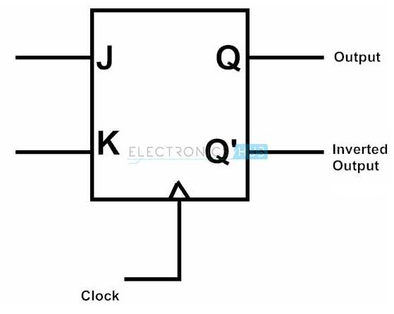
A JK flip – flop is the modification of SR flip – flop with no illegal state. In this the J input is similar to the SET input of SR flip – flop and the K input is similar to the RESET input of SR flip – flop. The symbol of JK flip – flop is shown below.
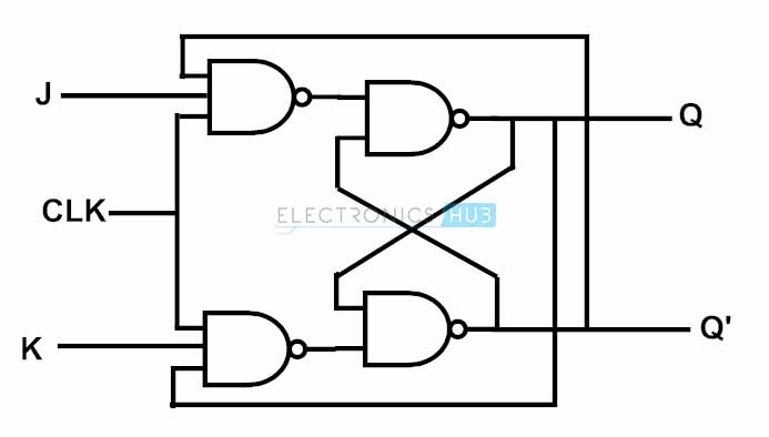
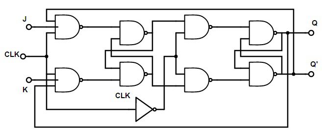
JK flip flop Logic Diagram
JK flip – flop logic diagram is shown in the below figure. As said before, JK flip – flop is a modified version of SR flip – flop. Logic diagram consists of three input NAND gates replacing the two input NAND gates in SR flip – flop and the inputs are replaced with J and K from S and R.
The design of the JK flip – flop is such that the three inputs to one NAND gate are J, clock signal along with a feedback signal from Q’ and the three inputs to the other NAND are K, clock signal along with a feedback signal from Q. This arrangement eliminates the indeterminate state in SR flip – flop.
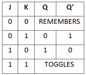
Truth Table
JK FlipFlop Operation
-
Case 1 : When both the inputs J and K are LOW, then Q returns its previous state value i.e. it holds the previous data.
When we apply a clock pulse to the J K flip flop and the J input is low then irrespective of the other NAND gates, the NAND gate-1 output becomes HIGH. In the same manner, if the K input is low then output of NAND gate-2 is also HIGH. So thus the output remains in the same state i.e. no change in the state of flip flop.
-
Case 2 : When J is LOW and K is HIGH, then flip flop will be in Reset state i.e. Q = 0, Q’ = 1.
When we apply a clock pulse to the J K flip flop and the inputs are J is low and K is high the output of the NAND gate connected to J input becomes 1. Then Q becomes 0. This will reset the flip flop again to its previous state. So the Flip flop will be in RESET state.
-
Case 3 : When J is HIGH and K is LOW, then flip – flop will be in Set state i.e. Q = 1, Q’ = 0
When we apply a clock pulse to the J K flip flop and the inputs are J is high and K is low the output of the NAND gate connected to K input becomes 1. Then Q’ becomes 0. This will set the flip flop with the high clock input. So the Flip flop will be in SET state.
-
Case 4 : When both the inputs J and K are HIGH, then flip – flop is in Toggle state. This means that the output will complement of the previous state.
Truth Table
The truth table of JK flip – flop is shown below.
Race around condition of JK Flip Flop
For high inputs of J K flip flop, only the lower NAND gates are triggered by the outputs that are compliment to each other i.e Q and Q’. So while high inputs are connected to flip – flop, at any instant, one gate is enabled and other gate will be disabled. If the upper gate is in disabled state, it will drive the flip flop to SET state, later when the lower gate is enabled, it will drive the flip flop to RESET state which causes the toggling of output. This will cause the Race around condition in J K flip – flop.
Steps to avoid racing condition
- We can avoid the Race around condition by setting up the clock-on time less than the propagation delay of the flip flop. It can be achieved by edge triggering.
- By making the flip flop to toggle over one clock period. This concept is introduced in Master Slave J K flip flop.
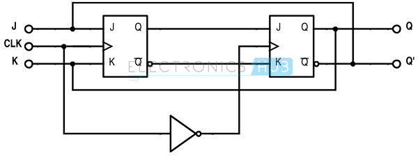
Master-Slave JK Flip Flop
The Master-Slave J K Flip flop is a “Synchronous” device which allows the data to pass with the timing of the clock signal. A master – slave flip flop consists of two clocked flip – flops connected in series, which isolate the input from output and hence the terminology “master – slave”. Apart from eliminating the race around problem in normal JK flip – flops, a master – slave JK flip – flop can also imitate the functions of SR flip – flop, clocked flip – flop, D flip – flop and Toggle flip – flop. The Q and Q’ outputs of the slave flip – flop are fed back to the master flip – flop while the outputs of the master flip – flop are connected as one of the inputs to the slave flip – flop.
When the clock input is high, the master is active and the slave is inactive. Depending on the inputs, the output of the master flip – flop is set or reset and the output of the slave flip flop is not changed and so it remains in previous state. As the slave flip flop become active at low clock input, the outputs of slave flip – flop changes. When the clock is high, the output of the master flip – flop are put on hold as the slave is inactive during this period. When the clock is low, the output of the master flip – flop are seen by the slave flip – flop and pass them to the output. The output of the slave flip flop is the final output of the Master – Slave flip – flop. The final output is available at the end of the clock pulse.
Construction
A master slave JK flip – flop is a cascaded combination of two SR flip – flops with the feedbacks from output of the slave to the input of the master. The circuit of master – slave flip – flop is shown below
Positive clock pulses are applied to the master flip flop and they are inverted before applying to slave i.e. master flip – flop is active during positive transition while slave flip – flop is active during negative transition. During the positive edge of the clock, the data from inputs J and K are passed to the master flip – flop and are held there till the occurrence of negative edge transition of the clock. Then the data or information is passed to the slave flip – flop, here the output is collected.
The symbolic representation of a master – slave JK flip – flop with two JK flip – flops is shown below.
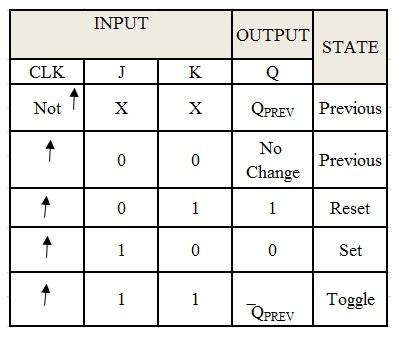
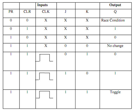
The truth table of master – slave JK flip – flop along with preset and clear inputs is shown below.
When the clock input is low, and the two inputs of master flip flop i.e. J and K inputs will have no effect on the output of Master Slave flip flop.
When the clock input is high
- If J is low & K is low: No change in state.
- If J is low & K is high: Master Slave flip flop will be in reset state.
- If J is high & K is low: Master Slave flip flop will be in set state.
- If J is high & K is high: Toggled state.
Timing Diagram
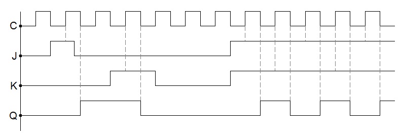
The width of the input pulse may be less or more than the propagation delay of the flip flop, it doesn’t affect the output state. But the value of J and K inputs at the instance of positive edge of clock will affect the output state of master – slave flip – flop provided the setup and hold time are not violated.
JK FlipFlop Applications
JK flip – flops are one of the most widely used flip – flops in digital electronics. This is because of their universal programmable feature.
Some of the applications of JK flip – flop include
• Shift Registers
• Frequency Dividers
• Switching Applications
• Parallel Data Transfer
• Serial Data Transfer
• Binary Counter
• Sequence Detector
One of the applications of JK flip flop is switching. This is explained below.
JK Flip Flop Switching
When we apply a clock signal to the JK flip – flop, the positive transition of the input clock signal enables the switching of present sate output. This enable condition does not continue through-out the positive cycle of the clock signal. The J and K inputs of the flip – flop cannot cause the transition of the clock pulse. But the input values at the time of positive transition will determine the output depending on their values. This is one of the applications of JK flip – flop. The output behavior of the JK flip – flop for the positive going transition on the clock is shown below with the help of wave forms
