In this tutorial, we will learn about a special type of Thyristor called the Gate Turn Off Thyristor. We will learn its construction, circuit symbol, the V-I Characteristics, the principle of operation and some of the commonly known applications of Gate Turn Off Thyristor.
Introduction
Although the thyristor is extensively used in high power applications, it always suffered from being a semi-controlled device. Even though it could be switched ON by applying a gate signal, it has to be turned OFF by interrupting the main current using a commutation circuit.
In case of DC to DC and DC to AC conversion circuits, this becomes a serious deficiency with thyristor due to the absence of natural current zero (as in case of AC circuits). Hence, the development of Gate Turn off Thyristor (GTO) addresses the major problem of the thyristor by ensuring the turn OFF mechanism through the gate terminal.

Basics of Gate Turn-Off Thyristor
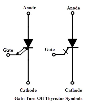
A Gate Turn off Thyristor or GTO is a three terminal, bipolar (current controlled minority carrier) semiconductor switching device. Similar to conventional thyristor, the terminals are anode, cathode and gate as shown in figure below. As the name indicates, it has gate turn off capability.
These are capable not only to turn ON the main current with a gate drive circuit, but also to turn it OFF. A small positive gate current triggers the GTO into conduction mode and also by a negative pulse on the gate, it is capable of being turned off. Observe in below figure that the gate has double arrows on it which distinguish the GTO from normal thyristor. This indicates the bidirectional current flow through the gate terminal.
The gate current required to turn off the GTO is relatively high. For example, a GTO rated with 4000V and 3000A may need -750A gate current to switch it off. So the typical turn off gain of GTO is low and is in the range of 4 to 5. Due to this large negative current, GTOs are used in low power applications.
On the other hand, during the conduction state GTO behaves just like a thyristor with a small ON state voltage drop. The GTO has faster switching speed than the thyristor and has higher voltage and current ratings than the power transistors.
Several varieties of GTOs are available in today’s market with asymmetric and symmetric voltage capabilities. GTOs with identical forward and reverse blocking capabilities are called as symmetric GTOs (S-GTOs). These are used in current source inverters, but these are somewhat slower. Mostly asymmetric GTOs (A-GTOs) are used due to its lower ON state voltage drop and stable temperature characteristics.
These asymmetrical GTOs have an appreciable reverse voltage capability (typically 20 to 25 V). These are used where either the reverse voltage across it would never occur or a reverse conducting diode is connected across the circuit. This article describes only about asymmetric GTOs.
Construction
Consider the below structure of GTO, which is almost similar to the thyristor. It is also a four layer, three junction P-N-P-N device like a standard thyristor. In this, the n+ layer at the cathode end is highly doped to obtain high emitter efficiency. This result the breakdown voltage of the junction J3 is low which is typically in the range of 20 to 40 volts.
The doping level of the p type gate is highly graded because the doping level should be low to maintain high emitter efficiency, whereas for having a good turn OFF properties, doping of this region should be high. In addition, gate and cathodes should be highly interdigited with various geometric forms to optimize the current turn off capability.
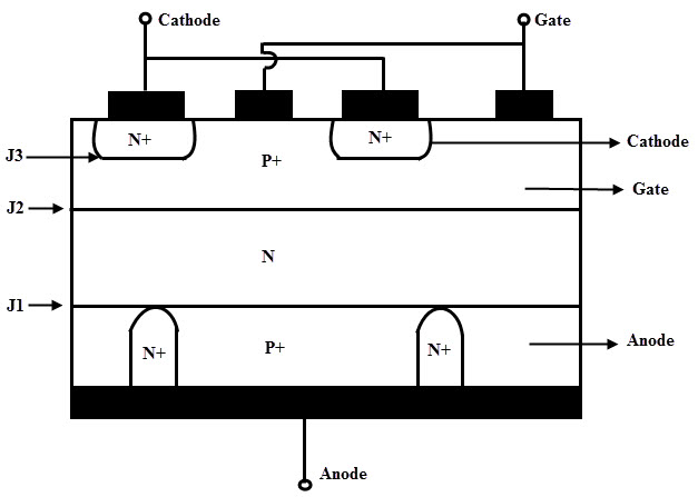
The junction between the P+ anode and N base is called anode junction. A heavily doped P+ anode region is required to obtain the higher efficiency anode junction so that a good turn ON properties is achieved. However, the turn OFF capabilities are affected with such GTOs.
This problem can be solved by introducing heavily doped N+ layers at regular intervals in P+ anode layer as shown in figure. So this N+ layer makes a direct contact with N layer at junction J1. This cause the electrons to travel from base N region directly to anode metal contact without causing hole injection from P+ anode. This is called as a anode shorted GTO structure.
Due to these anode shorts, the reverse blocking capacity of the GTO is reduced to the reverse breakdown voltage of junction j3 and hence speeds up the turn OFF mechanism.
However, with a large number of anode shorts, the efficiency of the anode junction reduces and hence the turn ON performance of the GTO degrades. Therefore, careful considerations have to be taken about the density of these anode shorts for a good turn ON and OFF performance.
Principle of Operation
The turn ON operation of GTO is similar to a conventional thyristor. When the anode terminal is made positive with respect to cathode by applying a positive gate current, the hole current injection from gate forward bias the cathode p-base junction.
This results in the emission of electrons from the cathode towards the anode terminal. This induces the hole injection from the anode terminal into the base region. This injection of holes and electrons continuous till the GTO comes into the conduction state.
In case of thyristor, the conduction starts initially by turning ON the area of cathode adjacent to the gate terminal. And thus, by plasma spreading the remaining area comes into the conduction.
Unlike a thyristor, GTO consists of narrow cathode elements which are heavily interdigitated with gate terminal, thereby initial turned ON area is very large and plasma spreading is small. Hence the GTO comes into the conduction state very quickly.
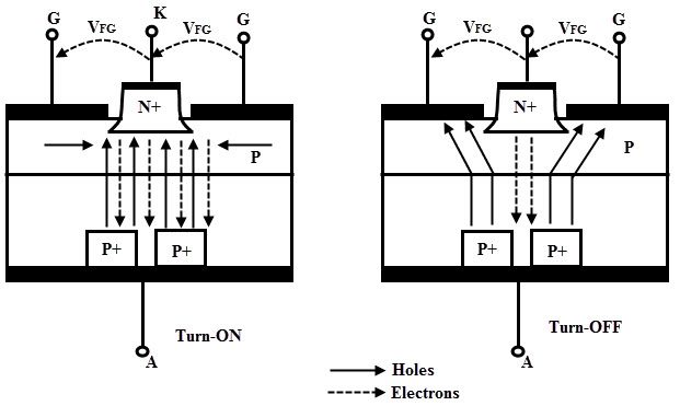
To turn OFF a conducting GTO, a reverse bias is applied at the gate by making the gate negative with respect to cathode. A part of the holes from the P base layer is extracted through the gate which suppress the injection of electrons from the cathode.
In response to this, more hole current is extracted through the gate results more suppression of electrons from the cathode. Eventually, the voltage drop across the p base junction causes to reverse bias the gate cathode junction and hence the GTO is turned OFF.
During the hole extraction process, the p-base region is gradually depleted so that the conduction area squeezed. As this process continuous, the anode current flows through remote areas forming high current density filaments. This causes local hot spots which can damage the device unless these filaments are extinguished quickly.
By the application of high negative gate voltage these filaments are extinguished rapidly. Due to the N base region stored charge, the anode to gate current continues to flow even though the cathode current is ceased. This is called a tail current which decays exponentially as the excess charge carriers are reduced by the recombination process. Once the tail current reduced to a leakage current level, the device retains its forward blocking characteristics.
V-I Characteristics
During the turn ON, GTO is similar to thyristor in its operates.So the first quadrant characteristics are similar to the thyristor. When the anode is made positive with respect to cathode, the device operates in forward blocking mode. By the application of positive gate signal triggers the GTO into conduction state.
The latching current and forward leakage currents are considerably higher in GTO compared to the thyristor as shown in figure. The gate drive can be removed if the anode current is above the holding current level.
But it is recommended not to remove the positive gate drive during conduction and to hold at value more than the maximum critical gate current. This is because the cathode is subdivided into small finger elements as discussed above to assist the turn OFF process.
This causes the anode current dips below the holding current level transiently, which forces a high anode current at a high rate back into the GTO. This can be potentially destructive. Therefore, some manufacturers recommend the continuous gate signal during the conduction state.
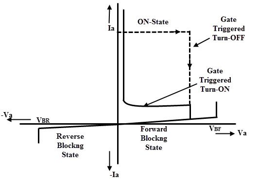
The GTO can be turned OFF by the application of reverse gate current which can be either step or ramp drive. The GTO can be turned OFF without reversing anode voltage. The dashed line in the figure shows i-v trajectory during the turn OFF for an inductive load. It should be noted that during the turn OFF, GTO can block a rated forward voltage only.
To avoid dv/dt triggering and protect the device during turn OFF, either a recommended value of resistance must be connected between the gate and cathode or a small reverse bias voltage (typically -2V) must be maintained on the gate terminal. This prevents the gate cathode junction to become forward biased and hence the GTO sustains during the turn OFF state.
In reverse biased condition of GTO, the blocking capability is depends on the type of GTO. A symmetric GTO has a high reverse blocking capability while asymmetric GTO has a small reverse blocking capability as shown in figure.
It is observed that, during reverse biased condition, after a small reverse voltage (20 to 30 V) GTO starts conducting in reverse direction due to the anode short structure. This mode of operation does not destroy the device provided that the gate is negatively biased and the time of this operation should be small.
Gate Turn-Off Thyristor Applications
Due to the advantages like excellent switching characteristics, no need of commutation circuit, maintenance-free operation, etc makes the GTO usage predominant over thyristor in many applications. It is used as a main control device in choppers and inverters. Some of these applications are
- AC drives
- DC drives or DC choppers
- AC stabilizing power supplies
- DC circuit breakers
- Induction heating
- And other low power applications

2 Responses
Hi. I am designing an automatic heater control(turn on and off) using GTO and arduino. So how can I turn off the heater supplied with 220V and 30A ? or can you suggest a better switch instead?
GOOD