Full wave rectifier rectifies the full cycle in the waveform i.e. it rectifies both the positive and negative cycles in the waveform. We have already seen the characteristics and working of Half Wave Rectifier. This Full wave rectifier has an advantage over the half wave i.e. it has average output higher than that of half wave rectifier. The number of AC components in the output is less than that of the input.
The full wave rectifier can be further divided mainly into following types.
- Center Tapped Full Wave Rectifier
- Full Wave Bridge Rectifier
Center Tapped Full Wave Rectifier
Center tap is the contact made at the middle of the winding of the transformer.
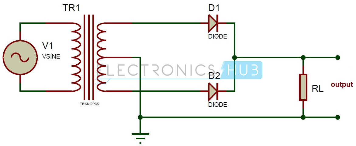
In the center tapped full wave rectifier two diodes were used. These are connected to the center tapped secondary winding of the transformer. Above circuit diagram shows the center tapped full wave rectifier. It has two diodes. The positive terminal of two diodes is connected to the two ends of the transformer. Center tap divides the total secondary voltage into equal parts.
Center Tapped Full Wave Rectifier Working:
The primary winding of the center tap transformer is applied with the Ac voltage. Thus the two diodes connected to the secondary of the transformer conducts alternatively. For the positive half cycle of the input diode D1 is connected to the positive terminal and D2 is connected to the negative terminal. Thus diode D1 is in forward bias and the diode D2 is reverse biased. Only diode D1 starts conducting and thus current flows from diode and it appears across the load RL. So positive cycle of the input is appeared at the load.
During the negative half cycle the diode D2 is applied with the positive cycle. D2 starts conducting as it is in forward bias. The diode D1 is in reverse bias and this does not conduct. Thus current flows from diode D2 and hence negative cycle is also rectified, it appears at the load resistor RL.
By comparing the current flow through load resistance in the positive and negative half cycles, it can be concluded that the direction of the current flow is same. Thus the frequency of rectified output voltage is two times the input frequency. The output that is rectified is not pure, it consists of a dc component and a lot of ac components of very low amplitudes.
Peak Inverse Voltage (PIV) of Centre Tap Full Wave Rectifier:
PIV is defined as the maximum possible voltage across a diode during its reverse bias. During the first half that is positive half of the input, the diode D1 is forward bias and thus conducts providing no resistance at all. Thus, the total voltage Vs appears in the upper-half of the ac supply, provided to the load resistance R. Similarly, in the case of diode D2 for the lower half of the transformer total secondary voltage developed appears at the load. The amount of voltage that drops across the two diodes in reverse bias is given as
PIV of D2 = Vm + Vm = 2Vm
PIV of D1 = 2Vm
Vm is the voltage developed across upper and lower halves.
Peak Current
The peak current is the instantaneous value of the voltage applied to the rectifier. It can be written as
Vs = Vsm Sinwt
Let us assume that the diode has a forward resistance of RF ohms and a reverse resistance is equal to infinity, thus current flowing through the load resistance RL is given as
Im = Vsm / (RF + RL)
Output Current
Since the current is same through the load resistance RL in the two halves of the ac cycle, magnitude of dc current Idc, which is equal to the average value of ac current, can be obtained by integrating the current i1 between 0 and pi or current i2 between pi and 2pi.
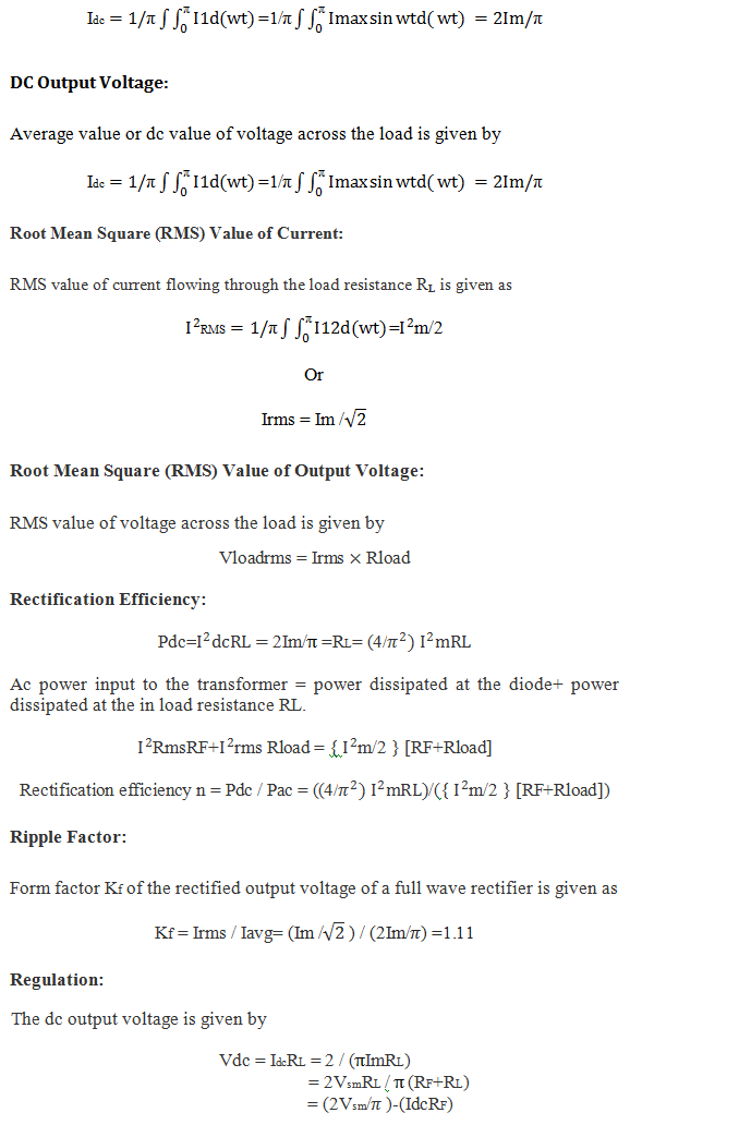
Transformer Utilization Factor:
This can be calculated by considering primary and secondary windings separately. Its value is 0.693.This can be used to determine transformer secondary rating.
Full Wave Bridge Rectifier
As the center tapped transformer is expensive and is difficult to implement bridge rectifier was developed. In this four diodes are arranged in the form of a bridge. This configuration provides same polarity output with either polarity. These two differ in PIV as the center tapped full wave rectifier produces an output voltage of Vm and bridge rectifier produces an output voltage of 2Vm. For more detailed information about Full wave rectifier circuit diagram, working and applications, read the post Full Wave Bridge Rectifier.

14 Responses
i cannot understand there r 2 types of fullwave rectifier
there are two types that are
1.using 2 diodes
and 2. using 4 diodes i.e bridge rectifier
Thank you
a very helpful site and information along with working and diagram makes it very efficient..!
Ok ,good.bt add some equations
I cannot understand
In the calculation you took pi in the base but this base that is pi only for half cycle. The full base is 2*pi. Then what will be Idc for for the base 2*pi?
In the calculation you took pi in the base but this base that is pi only for half cycle. The full base is 2*pi. Then what will be Idc for for the base 2*pi??
this is very meaning ful theory,and in very simple language to understand very easily
thank u
I need input and output wave forms of center tapped FWR
i need appropriate notes for full wave rectifier with filter.
this is very helpful to every one and is in a simple language so that anyone can understand.Thank you
Plz change the sentences of brize type full wave rectifier and some new easy sentence which can be understand.
Very nice