A Flip – flop is an electronic device which is having two stable states and a feedback path which is used to store 1 – bit of information by using the clock signal as input. Latches are also used to do the same task except that they do not use a clock signal. Hence to say it simply, “Flip – flops are clocked latches”. They are used to store only 1 – bit of information and it can remain in the same state until the clock signal affects the state of the input.
There are four types of flip – flops
- SR flip – flop
- D flip – flop
- JK flip – flop
- T flip – flop
FlipFlop Conversions
Generally, JK flip – flops and D flip – flops are the most widely used flip – flops. And so their availability in the form of integrated circuits (IC’s) is abundant. Numerous varieties of JK flip – flop and D flip – flop are available in the semiconductor market. The less popular SR flip – flop and T flip – flop are not available in the market as integrated circuits (IC’s) (even though a very few number of SR flip – flops are available as IC’s, they are not frequently used).
There might be a situation where the less popular flip – flops are required in order to implement a logic circuit. In order use the less popular flip – flops, we will convert one type of flip – flop into another. Some of the most common flip – flop conversions are
- SR Flip – flop to JK Flip – flop
- SR Flip – flop to D Flip – flop
- SR Flip – flop to T Flip – flop
- JK Flip – flop to SR Flip – flop
- JK Flip – flop to D Flip – flop
- JK Flip – flop to T Flip – flop
- D Flip – flop to SR Flip – flop
- D Flip – flop to JK Flip – flop
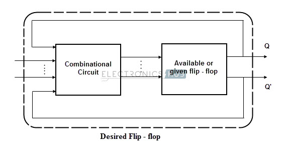
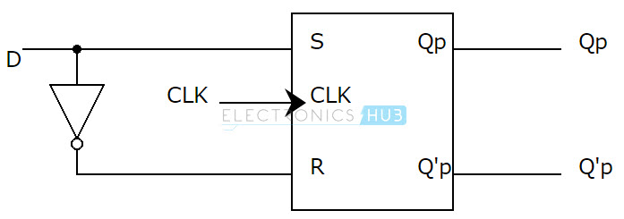
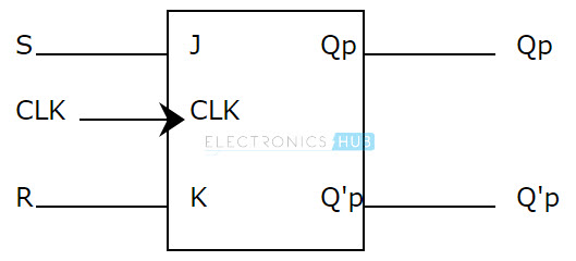
In order to convert one flip – flop to other type of flip – flop, we should design a combinational circuit that is connected to the actual flip – flop. Inputs to combinational circuit are same as the inputs of the desired flip – flop. Outputs of combinational circuit are same as the inputs of the available flip – flop. So the output of combinational circuit is connected to the input of our available flip – flop. The pictorial representation of the same is shown below.
SR Flip – flop to other Flip – flops
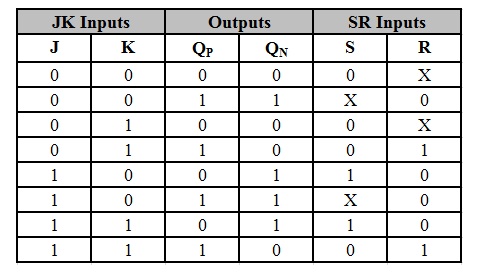
SR Flip – flop to JK Flip – flop
Here we are required to convert the SR flip – flop to JK flip – flop. So first we design a combinational circuit with J and K as its inputs and we connect its output to the input of our available flip flop i.e. an SR flip – flop. So its outputs are same as that of JK flip – flop.
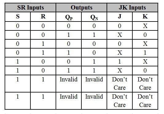
Let’s write a truth table for the two inputs, J and K. For two inputs along with the QP, we get 8 possible combinations in truth table. Consider that when the two inputs are applied, QP is the present state and QN is the next state. For every combination of J, K ,QP , we find the corresponding QN state. Here QN will give the state values that to which the output of the JK flip – flop will jump after the present state, on applying the inputs. Now we write all the combinations of S and R in the truth table to get each QN value from corresponding QP. Hence these are the values of S and R that are used to change the state of flip flop from QP to QN.
The conversion table from SR flip – flop to JK flip – flop is shown below.
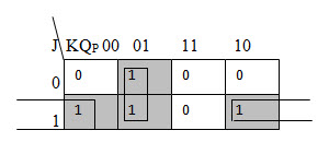
In order to deduce the Boolean equations of S and R in terms of J and K, we use Karnaugh maps from the above table.
The K – map for S is shown below.

The Boolean equation for S is S = JQ’P.
The K – map for R is shown below.

The Boolean equation for R is R = KQP.
The Boolean equations of S and R in terms of J, K and QP are: S = JQ’P and R = KQP
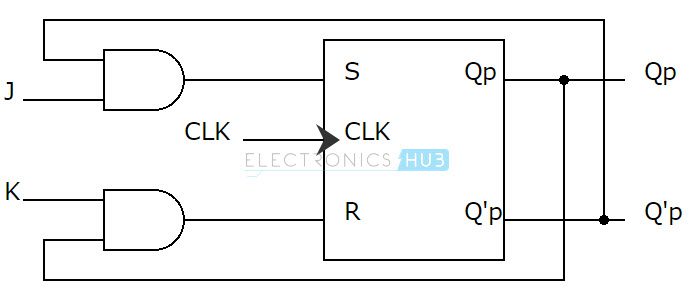
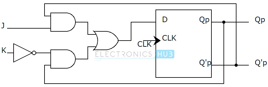
The logic diagram of JK flip – flop implemented from SR flip – flop is shown below. Here J and K are external inputs to the circuit. S and R are the outputs of the designed combinational outputs.
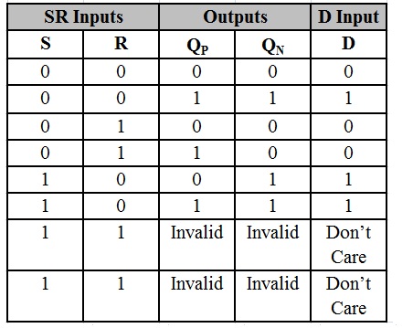
SR Flip – flop to D Flip – flop
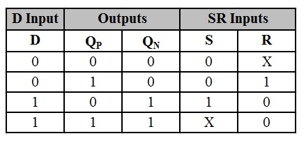
Converting the SR flip – flop to D flip – flop involves connecting the Data input (D) to the SR flip – flop. Here the Data input is connected directly to the S input and the inverted D input (using a NOT gate) is connected to R input. The same can be derived from truth table and corresponding K – maps. S and R are the inputs of the flip – flop while QP and QP’ are the present state and its complementary outputs of the flip – flop. We should design a combinational circuit such that its input is D and outputs are S and R. Outputs from the combinational circuit S and R are connected as inputs to the SR flip – flop.
The truth table for conversion of SR flip – flop to D flip – flop is shown below. The truth table is drawn for the D input and QP output to find the corresponding QN output.
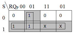
The K – map to derive the Boolean equation of S in terms of D is shown below.
The Boolean equation of S is S = D.
The K – map to derive the Boolean equation of R in terms of D is shown below.
The Boolean equation of R is R = D’.
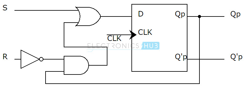
The Boolean equation for S and R in terms of D are: S = D and R = D’. The logic diagram of implementation of D flip – flop from SR flip – flop is shown below.
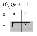
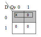
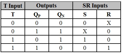
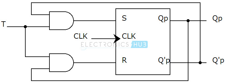
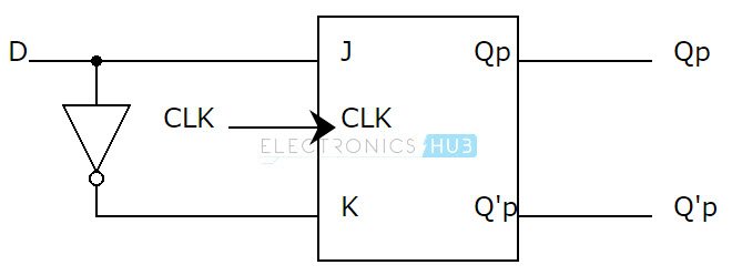
SR Flip – flop to T Flip – flop
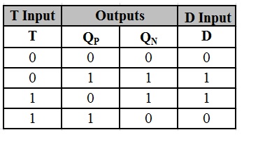
The combinational circuit required in order to convert an SR flip – flop to T flip – flop can be constructed from the truth table. The input to the combinational circuit is T (Toggle input) and the outputs of the combinational circuit are S and R. Here S and R are the inputs of the actual flip – flop. The output and the complement output of the flip – flop are QP and Q’P. The truth table consists of combinations of T and QP in order to get QN where QN is the next state output of the flip – flop. The combinations of S and R which results in QN are also tabulated in the same table.
The conversion table is shown below.
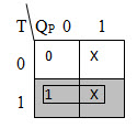
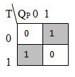
The K – map to derive the Boolean equation of S in terms of T and QP is shown below.
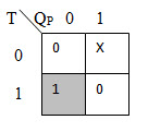
The Boolean equation of S is S = TQ’P.
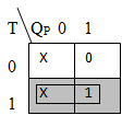
The K – map to derive the Boolean equation of R in terms of T and QP is shown below.
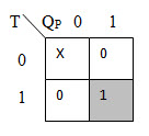
The Boolean equation for R is R = TQP.
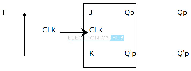
The Boolean equations of S and R are: S = TQ’P and R = TQP. The logic circuit for the implementation of T flip – flop from SR flip – flop is shown below.
JK Flip – flop to other Flip – flops
JK Flip – flop to SR Flip – flop
To convert the JK flip – flop into SR flip – flop, we design a combinational circuit with S and R as its inputs and J and K as its outputs. Here J and K are the inputs of actual flip – flop. So for making this conversion, we should obtain the J &, K values in terms of S, R and QP.
Consider that when the two inputs S and R are applied, QP is the present state output and QN is the next state output. For each combination of S, R and QP, we find the corresponding QN state.
Now, we prepare a truth table for the possible combination of the inputs S, R and QP. We can make 8 possible combinations for the two S and R inputs along with QP. For each combination of S and R inputs and QP we find the corresponding value of QN. Now we write all the values of J and K in the truth table to get each QN value from corresponding QP.
In SR flip – flop, when the 2 inputs are high i.e. S = 1 & R = 1, then the flip – flop will be in undefined state or forbidden state. So for this combination we consider the J, K inputs as ‘Don’t cares’.
The conversion table for implementing SR flip – flop from JK flip – flop is shown below.
The K – map for J is shown below.

The Boolean equation for J is J = S.
The K – map for K is shown below.

The Boolean equation for K is K = R.
The Boolean equations for J and K in terms of S and R are: J = S and K = R. Hence, there is no requirement of any additional combinational circuit as S and R inputs are same as J and K inputs. The logic circuit of implementing SR flip – flop from JK flip – flop is shown below.
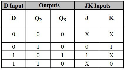
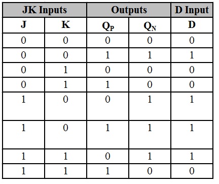
JK Flip – flop to D Flip – flop
Converting the JK flip – flop to D flip – flop, involves in connecting the Data input (D) to the JK flip – flop through a combinational circuit. Here the Data input is connected directly to the J input and the inverted D input (using a NOT gate) is connected to K input.
The design of the combinational circuit should be in such a way that D is its input and J & K are its outputs. The outputs of the combinational circuit J & K are connected as inputs to the flip – flop. QP is the present state output of the flip – flop. Q’P is its complementary and QN is the next state output. The truth table for converting JK flip – flop to D flip – flop is shown below.
The K – maps in order to solve for J and K in terms of D and QP are shown below.
K – Map for J.
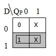
The Boolean equation for J is J = D.
K – Map for K.
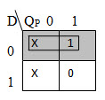
The Boolean equation for K is K = D’.
The Boolean equations for J and K are J = D and K = D’. The logic diagram that represents the implementation of D flip – flop from JK flip – flop is shown below.
JK Flip – flop to T Flip – flop
Converting the JK flip – flop to T flip flop, involves in connecting the Toggle input (T) directly to the J and K inputs. So toggle (T) will be the external input to the combinational circuit. Its output is connected to the Input of actual flip – flop (JK flip – flop).
We prepare a truth table by considering 4 possible combinations of the Toggle input (T) along with QP. QP and QP’ are the present state output and its complement output of the flip – flop. QN is the next state output. The truth table is drawn for the T input and QP output to find the corresponding QN output.
The truth table is shown below.

The K – map for solving the Boolean equations of J in terms of T and QP is shown below.
The Boolean equation for J is J = T.
The K – map for solving the Boolean equations of K in terms of T and QP is shown below
The Boolean equation for K is K = T.
The logic circuit for converting JK flip – flop to T flip – flop is shown below.
D Flip – flop to other Flip – flops
D Flip – flop to SR Flip – flop
To convert the D flip – flop into SR flip – flop, a combinational circuit should be constructed where its inputs are S and R and its output is D. Here Data (D) is the input of actual flip – flop. The truth table is drawn with the 8 possible combinations of the two inputs S & R and QP. QP and QP’ are the present state and its complement outputs of the flip – flop.
When the two inputs of SR flip – flop are high i.e. S = 1 and R = 1, then the QP value is invalid and hence the Data (D) inputs for the corresponding QP’s are considered as ‘Don’t cares’.
The truth table for S, R and QP in order to get QN is shown below. It also consists of D inputs in order to get the same QN.
The K – map for solving the equation of D in terms of S, R and QP.
The Boolean equation of D is D = S + R’QP. The logic diagram using this equation to implement an SR flip – flop from D flip – flop is shown below.
D Flip – flop to JK Flip – flop
When we need to convert the D flip – flop into JK flip – flop, J and K are the inputs of the combinational circuit with D as its output. Here Data (D) is the input of actual flip – flop. The truth table is drawn with the 8 possible combinations of the two inputs J & K along with QP. QP and QP’ are the present state and its complement outputs of the flip – flop.
The truth table consists of combinations of J, K and QP in order to get QN. Here QN is the next state output of the flip – flop. The truth table also consists of D inputs that lead to QN output.
The conversion table is shown below.
The K – map implementation of D in terms of J, K and QP is shown below.
The Boolean equation of D deduced from the above K – map is D = JQ’P + K’QP. The logical representation of implementing JK flip – flop from D flip – flop is shown below.
D Flip – flop to T Flip – flop
When we need to convert the D flip – flop into T flip – flop, T (Toggle input) is the input of the combinational circuit with D as its output. Here Data (D) is the input of actual flip – flop. The truth table is drawn with the 4 possible combinations of the input T along with QP. QP and QP’ are the present state and its complement outputs of the flip – flop.
The truth table consists of combinations of T and QP in order to get QN. Here QN is the next state output of the flip – flop. The truth table also consists of D inputs that lead to QN output.
The conversion table is shown below.
The K – map for D is shown below.
The Boolean equation of D in terms of T and QP is D = T’QP + TQ’P. The logic circuit for implementing T flip – flop with D flip – flop is shown below.


One Response
Thank you for this useful information