Here I’m discussing about the topic FET. FET is another semiconductor device like BJT which can be used as switch, amplifier, resistor etc.
FET consists of 3 terminals.
- Drain(D)
- Source(S)
- Gate(G)
In these 3 terminals, Gate terminal acts as a controlling terminal. We know that a BJT acts as a current controlling device. Like that, FET also acts as a voltage controlling device. Here, the voltage between gate and source controls the drain current. So, it is called as voltage controlled device.
Field Effect Transistor (FET) Features:
- FET is more temperature stable compared to BJT
- It requires less space compared to BJT. So it is used heavily in circuits.
- FET has higher input impedance. So, it is more useful in amplifiers.
Types of FETs:
- Junction FET
- MESFET
- MOSFET
Here I am discussing about the topic JFET.
Junction FET (JFET): Basically the JFET is classified into 2 types.
- N-Channel JFET
- P-Channel JFET
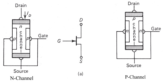
N-Channel JFET: When we consider a silicon bar and fabricated n-type at its two ends and heavily doped p-type materials at each side of the bar, the thin region will be remained as observed in figure is channel. Since this channel is in n-type bar this is called as n-channel FET. Here the current is carried by electrons.
P-Channel FET: When we consider a silicon bar and fabricated p-type at its two ends and heavily doped n-type materials at each side of the bar, here the thin region remained as observed in figure is channel. Since this channel is in n-type bar this is called as p-channel FET. Here the current is carried by holes.
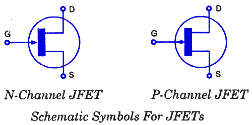
Symbols of N-channel JFET and P-channel JFET:
Biasing JFET:
Unbiased JFET: In the absence of any applied voltage, JFET has gate channel junctions under no bias conditions. The result is a depletion region at each junction as shown in figure.
Operation: In JFET the p-n junction between source and gate is always kept in reverse biased conditions. Hence, practically in reverse biased conditions the current is less (zero).
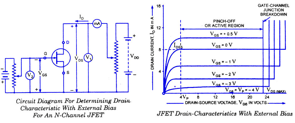
Consider N-Channel JFET with gate open and supply is applied between gate and source as shown in figure. Due to polarities of applied voltage, the majority carriers start flowing from source to the drain. The majority carriers basically move through the space between the gate regions. This space is known as channel. The width of channel can be controlled by varying the gate voltage. The effect of variation of width can be observed in following cases.
When we connected an N-Channel JFET with the gate directly connected to the source terminal. When drain voltage is applied, a drain current flows through channel. It causes a voltage drop across depletion region to penetrate into channel. Since gate is heavily doped and channel is lightly doped, the width of depletion region is spread into channel.
In the same way if we applied less voltage at the gate, we can get the depletion region as shown in figure and if we applied more voltage at the gate, we can get the depletion region which covers the entire channel without any gap. So there will be no current flow from drain to source through channel.
The gate to source voltage that produces cutoff is known as cutoff voltage.
V-I Charactaristics of N-Channel JFET:
Related Posts:
