In this transistor tutorial, we will learn about Different Configurations of Transistors. Since a Bipolar Junction Transistor is a 3-terminal device, there are three different configurations of Transistors possible with BJTs. Understanding these different configurations of transistors will help you in better implementation of your application.
Introduction
We know that generally the transistor has three terminals – emitter (E), base (B) and collector. But in the circuit connections we need four terminals, two terminals for input and another two terminals for output. To overcome these problems we use one terminal as common for both input and output actions.
Using this property we construct the circuits and these structures are called transistor configurations. Generally there are three different configurations of transistors and they are common base (CB) configuration, common collector (CC) configuration and common emitter (CE) configuration.
The behavior of these three different configurations of transistors with respect to gain is given below.
- Common Base (CB) Configuration: no current gain but voltage gain
- Common Collector (CC) Configuration: current gain but no voltage gain
- Common Emitter (CE) Configuration: current gain and voltage gain
Now we discuss about these three different configurations of transistors with their input and output characteristics in the below sections.
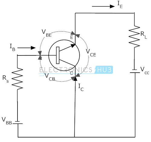
Common Base Configuration
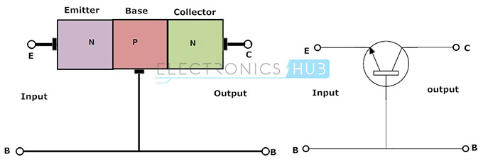
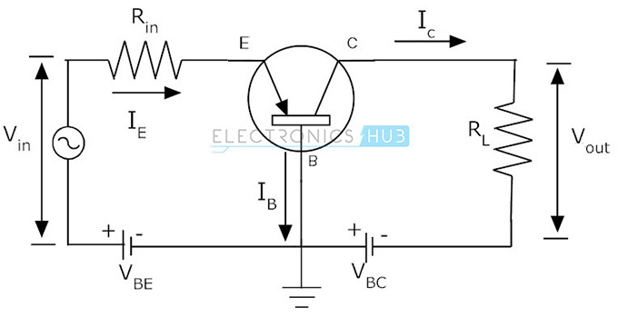
In this configuration we use base as common terminal for both input and output signals. The configuration name itself indicates the common terminal. Here the input is applied between the base and emitter terminals and the corresponding output signal is taken between the base and collector terminals with the base terminal grounded. Here the input parameters are VEB and IE and the output parameters are VCB and IC. The input current flowing into the emitter terminal must be higher than the base current and collector current to operate the transistor, therefore the output collector current is less than the input emitter current.
The current gain is generally equal or less than to unity for this type of configuration. The input and output signals are in-phase in this configuration. The amplifier circuit configuration of this type is called as non-inverting amplifier circuit. The construction of this configuration circuit is difficult because this type has high voltage gain values.
The input characteristics of this configuration are looks like characteristics of illuminated photo diode while the output characteristics represents a forward biased diode. This transistor configuration has high output impedance and low input impedance. This type of configuration has high resistance gain i.e. ratio of output resistance to input resistance is high. The voltage gain for this configuration of circuit is given below.
AV = Vout/Vin = (IC*RL) / (IE*Rin)
Current gain in common base configuration is given as
α = Output current/Input current
α = IC/IE
The common base circuit is mainly used in single stage amplifier circuits, such as microphone pre amplifier or radio frequency amplifiers because of their high frequency response. The common base transistor circuit is given below.
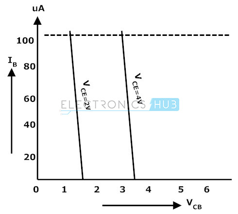
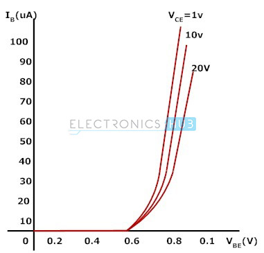
Input Characteristics
Input characteristics are obtained between input current and input voltage with constant output voltage. First keep the output voltage VCB constant and vary the input voltage VEB for different points then at each point record the input current IE value. Repeat the same process at different output voltage levels. Now with these values we need to plot the graph between IE and VEB parameters. The below figure show the input characteristics of common base configuration. The equation to calculate the input resistance Rin value is given below.
Rin = VEB / IE (when VCB is constant)

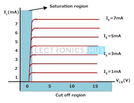
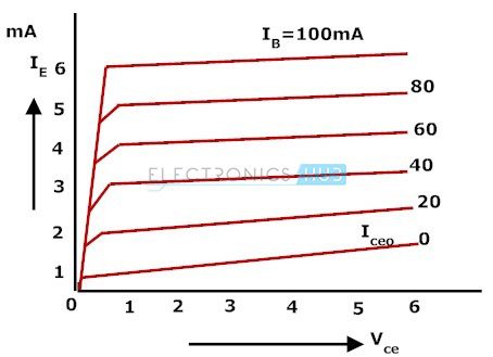
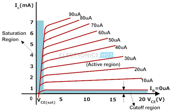
Output Characteristics
The output characteristics of common base configuration are obtained between output current and output voltage with constant input current. First keep the emitter current constant and vary the VCB value for different points, now record the IC values at each point. Repeat the same process at different IE values. Finally we need to draw the plot between VCB and IC at constant IE. The below figure show the output characteristics of common base configuration. The equation to calculate the output resistance value is given below.
Rout = VCB / IC (when IE is constant)
Common Collector Configuration
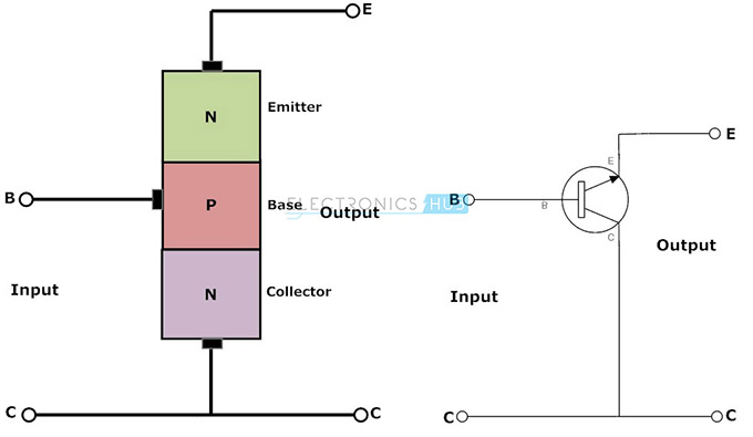
In this configuration we use collector terminal as common for both input and output signals. This configuration is also known as emitter follower configuration because the emitter voltage follows the base voltage. This configuration is mostly used as a buffer. These configurations are widely used in impedance matching applications because of their high input impedance.
In this configuration the input signal is applied between the base-collector region and the output is taken from the emitter-collector region. Here the input parameters are VBC and IB and the output parameters are VEC and IE. The common collector configuration has high input impedance and low output impedance. The input and output signals are in phase. Here also the emitter current is equal to the sum of collector current and the base current. Now let us calculate the current gain for this configuration.
Current gain,
Ai = output current/Input current
Ai = IE/IB
Ai = (IC + IB)/IB
Ai = (IC/IB) + 1
Ai = β + 1
The common collector transistor circuit is shown above. This common collector configuration is a non inverting amplifier circuit. The voltage gain for this circuit is less than unity but it has large current gain because the load resistor in this circuit receives both the collector and base currents.
Input Characteristics
The input characteristics of a common collector configuration are quite different from the common base and common emitter configurations because the input voltage VBC is largely determined by VEC level. Here,
VEC = VEB + VBC
VEB = VEC – VBC
The input characteristics of a common-collector configuration are obtained between inputs current IB and the input voltage VCB at constant output voltage VEC. Keep the output voltage VEC constant at different levels and vary the input voltage VBC for different points and record the IB values for each point. Now using these values we need to draw a graph between the parameters of VBC and IB at constant VEC.
Output Characteristics
The operation of the common collector circuit is same as that of common emitter circuit. The output characteristics of a common collector circuit are obtained between the output voltage VEC and output current IE at constant input current IB. In the operation of common collector circuit if the base current is zero then the emitter current also becomes zero. As a result no current flows through the transistor
If the base current increases then the transistor operates in active region and finally reaches to saturation region. To plot the graph first we keep the IB at constant value and we will vary the VEC value for various points, now we need to record the value of IE for each point. Repeat the same process for different IB values. Now using these values we need to plot the graph between the parameters of IE and VCE at constant values of IB. The below figure show the output characteristics of common collector.
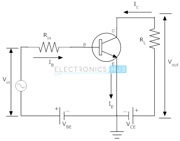
Common Emitter Configuration
In this configuration we use emitter as common terminal for both input and output. This common emitter configuration is an inverting amplifier circuit. Here the input is applied between base-emitter region and the output is taken between collector and emitter terminals. In this configuration the input parameters are VBE and IB and the output parameters are VCE and IC.
This type of configuration is mostly used in the applications of transistor based amplifiers. In this configuration the emitter current is equal to the sum of small base current and the large collector current. i.e. IE = IC + IB. We know that the ratio between collector current and emitter current gives current gain alpha in Common Base configuration similarly the ratio between collector current and base current gives the current gain beta in common emitter configuration.

Now let us see the relationship between these two current gains.
Current gain (α) = IC/IE
Current gain (β) = IC/IB
Collector current IC =α IE = βIB
This configuration is mostly used one among all the three configurations. It has medium input and output impedance values. It also has the medium current and voltage gains. But the output signal has a phase shift of 1800 i.e. both the input and output are inverse to each other.
Input Characteristics
The input characteristics of common emitter configuration are obtained between input current IB and input voltage VBE with constant output voltage VCE. Keep the output voltage VCE constant and vary the input voltage VBE for different points, now record the values of input current at each point. Now using these values we need to draw a graph between the values of IB and VBE at constant VCE. The equation to calculate the input resistance Rin is given below.
Rin = VBE/IB (when VCE is at constant)
Output Characteristics
The output characteristics of common emitter configuration are obtained between the output current IC and output voltage VCE with constant input current IB. Keep the base current IB constant and vary the value of output voltage VCE for different points, now note down the value of collector IC for each point. Plot the graph between the parameters IC and VCE in order to get the output characteristics of common emitter configuration. The equation to calculate the output resistance from this graph is given below.
Rout = VCE/IC (when IB is at constant)
Configurations of Transistors Summary
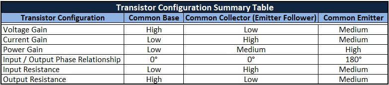
The table which gives the main characteristics of a transistor in the three configurations is given above. The BJT transistors have mainly three types of configurations. They are common-emitter, common-base and common-collector configurations. Among all these three configurations common-emitter configuration is mostly used type. These three have different characteristics corresponding to both input and output signals. And also these three configurations have few similarities.

34 Responses
i read this topic and i feel better but explanation of input & output characteristic is to loss
It’s the best summary.
Very good. Includes all the three configurations and its characteristics.
I want a simple transistor circuit for designing….
Can you explain why Vin is used when Vbe is present as an input voltage..?Vbe and Vcb are the input and output voltages..Then why the output is being taken across a resistor?
we use resistor,which is also called load resistor and without load resistor we cannot measure or indicate emitter current,because when we say current there must be a load otherwise there will be no current,input voltage Vin is written just for understanding purpose we can also write Veb
Can you explain the use of Vin as the input voltage when Vbe is present and why is there a need of taking output across a resistor? This question is with respect to Common Base Configuration circuit.
Describe the current voltage characteristics for the 3 configuration of a PNP transistor. Note not more than 4page
There is one mistake. I think voltage gain is low for common Base configuration
Very nicely explained thanks…
i think this can be better|try again
Yes it’s is an and easy to understand
well explained.
can someone give the expression for collector current in CB and CE configuration
I feel better to read this. And it gives me a lot of information. And i had a doubt What is meant by Non inverting amplifier circuit ??
It can be used for students and also better explained and I expect more.
PERFECT AND SHORT EXPLANATION FOR TRANSISTOR
Nicely expained.
Why we take Vce in input and Ib in output as constant in common emitter configuration??
The concept is very easy to understand in this site … I feel better ?
well explain at all,Great point in pn-junction
Super explanation
just clean…..loved it
best diagrambased explanation!
Most beautiful explaination so Thank u so much….
The details of breakdown region and knee voltage is missing in output characteristics of CE configuration
good bro
Thanks! THIS WAS THE ONLY SATISFACTORY EXPLANATION! I’m gonna get this printed:)
Saved day..! Thanks
thank youu
Sir it was awesome
The primitive idea of various configurtions are clearly shown
Thankyou for this….keep it up!?
Your article is detailed. It presents a great way to refresh my knowledge on Transistor configurations.