D flip – flops are also called as “Delay flip – flop” or “Data flip – flop”. They are used to store 1 – bit binary data. They are one of the widely used flip – flops in digital electronics. Apart from being the basic memory element in digital systems, D flip – flops are also considered as Delay line elements and Zero – Order Hold elements.
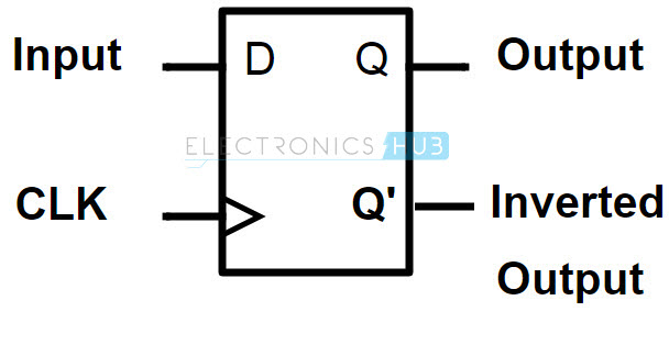
D flip – flop has two inputs , a clock (CLK) input and a data (D) input and two outputs; one is main output represented by Q and the other is complement of Q represented by Q’. The symbol of a D flip – flop is shown below.
D Flip Flop Construction
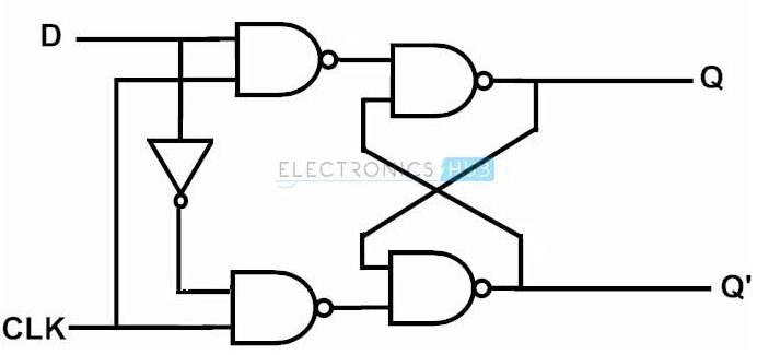
A D flip – flop is constructed by modifying an SR flip – flop. The S input is given with D input and the R input is given with inverted D input. Hence a D flip – flop is similar to SR flip – flop in which the two inputs are complement to each other, so there will be no chance of any intermediate state occurs. The major drawback of SR flip – flop is the race around condition which in D flip – flop is eliminated (because of the inverted inputs). The circuit diagram of D flip – flop is shown in below figure.
D Flip Flop Working
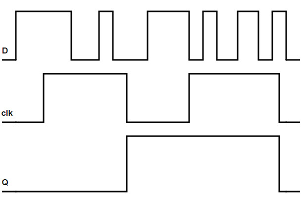
When we don’t apply any clock input to the D flip flop or during the falling edge of the clock signal, there will be no change in the output. It will retain its previous value at the output Q. If the clock signal is high (rising edge to be more precise) and if D input is high, then the output is also high and if D input is low, then the output will become low. Hence the output Q follows the input D in the presence of clock signal.
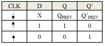
Simply, for positive transition on clock signal,
If D = 0 => Q = 0 so flip flop is reset.
If D = 1 => Q = 1 so flip flop is set.
NOTE: ↑ indicate positive edge of the clock and ↓ indicate negative edge of the clock signal.
Edge triggered D flip flop
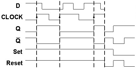
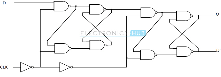
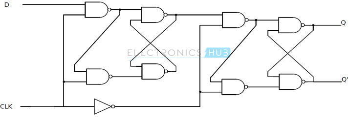
The positive edge triggered D flip flop is constructed from three SR NAND latches. Input stage consists of two latches and the output stage consists of one latch. At the input stage, a data input is connected to one of NAND latches and a clock signal (CLK) is connected to both the SR latches in parallel.
The operation can be explained as follows, when clock signal is low, the outputs of input stage are at high logic irrespective of the value on the data input. Hence, the previous data it stored. When clock is going through a positive transition ( low to high ) , the outputs of the input stage are responsible for set or reset operation of the final output and are dependent on data signal. If the data input is high, the output of the upper latch becomes low and thus sets the latch output to 1 and if the data input is low, the output of the lower latch becomes low which resets the output to 0. If the clock is continuously high for multiple data signals, only the first data input is considered while the remaining data inputs are ignored by forcing output latch to its previous state , as the low input is active as long as clock signal is high. Therefore, the outer latch stores data only when clock is at low logic . The main role of the triggered D flip flop is to hold the output till the clock pulse changes from low to high. The timing diagram of edge triggered D flip – flop is shown below.
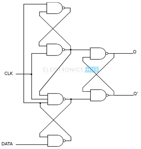
Master Slave D Flip Flop
Master slave D flip flop can be designed by the series connection of two gated D latches and connecting an inverted enable input either to of the two latches. Only the change in Master latch will bring change in Slave latch. So these are called Master Slave flip flops. The total circuit of master slave flip flop is triggered either on the rising edge of the clock signal or on falling edge of clock signal depending on the design.
The symbolic representation of a master slave D flip flop that responds to the clock at its falling edge as shown below.
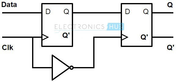
The Master slave D flip flop shown below is a positive edge triggered device that means it will operate when clock input has raising edge. The first flip flop (master flip – flop) is connected with a negative clock signal i.e inverted and the second flip – flop (slave flip – flop) is connected with double inverse of clock signal i.e. normal clock signal.
D Flip Flop Operation
The operation of positive edge triggered Master Slave D flip flop is explained below.
- If clock is low, the enable signal to master flip flop is high. When clock signal changes from low to high, the master flip flop stores the data from the D input. Simultaneously at the second flip flop , the enable signal goes low to high along with clock signal because of the double inversion. The data locked by the master flip flop during the rising edge are passed to the slave flip flop.
- When clock signal goes high to low, the slave flipflop will receive the master flip flop output as its input and changes its state. Master flipflop will accept latest values from the inputs on next rising edge.
The timing diagram of master slave D flip flop is shown below.
A simple modification will turn the above device in to negative edge triggering device. A negative edge triggered master slave D flip flop is formed by eliminating first inverter along the clock signal path.
D Flip Flop Applications
D flip – flops are one of the most widely used flip – flops. Some of the many applications of D flip – flop are
- Data storage registers.
- Data transferring as shift registers.
- Frequency division circuits.
D Flip Flop Data Storage
In digital circuits the data is normally stored as a group of bits, represented in numbers and codes. So it is easy to take data on parallel lines and store the data simultaneously in a group of flip flops, arranged in a particular order.. Registers are the basic multi – bit data devices. They are formed by connecting number of D flip – flops such that multiple bits of data can be stored.
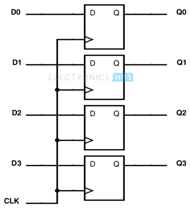
Each D flip – flop is connected with a respective data input. Clock input applied is same to all the flip – flops so that all of them will store the data simultaneously from their respective D inputs when a positive edge triggered clock signal is applied.
Data Transfer
D flip – flops are also widely used in data transfer. For transferring the data, D flip – flops are connected to form a shift register. A cascade connection of D flip – flops with same clock signal will form a shift register. A shift register can shift the data without changing the sequence of bits. When a clock pulse is applied, the one bit data is shifted or transferred. Shift registers can store the data temporarily.
The 4 bit storage shift register using D flip flop is shown below.
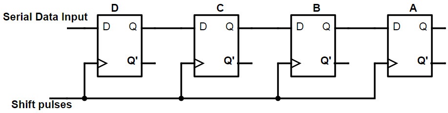
Shift registers are used in serial to parallel and parallel to serial data conversion. They are also used as pulse extenders and delay circuits.
Frequency Division Using D Flip Flop
Frequency Division circuits are developed by using D flip flops. This is the most important application of D Flip Flop. In Frequency Division circuits the state output of the D flip flop (Q’) is connected to the Data input (D) as a closed feedback loop. Two successive cock pulses will make the flip flop to Toggle, for every two clock cycles.
As the name implies, the frequency divider circuits are used to produce the digital signal output exactly half the input frequency. The frequency divider circuits are generally used in design of asynchronous counters.
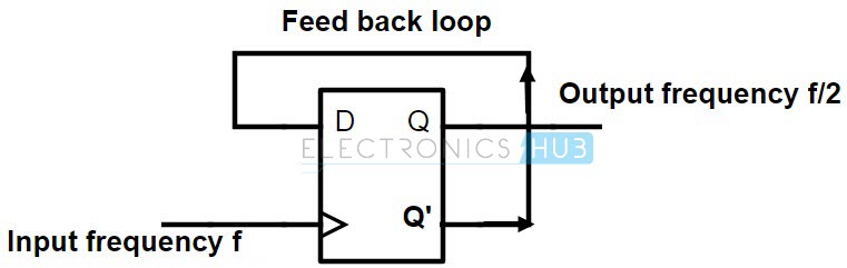
The operation of the circuit is very simple. The incoming data signal is clocked by the clock input signal. The circuit will perform the division of the input frequency by using the feedback loop i.e. connected to the Data input from Q’. The frequency divider circuit divides the input frequency by 2 for every two clock pulses.
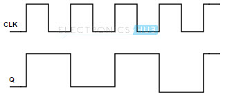
It can be explained by using the output compared with the clock signal.
In a situation, when Q output is 1, Q’ output is 0, then the data from the D input is clocked through the Q output on the next positive going edge of clock input signal. At this instance the output changes from high to low. Here the output remains same until the occurrence of next positive clock signal. Similarly the Q’ output is also clocked. As the clock input is 1 again, this will change the output state of flip flop.
We can observe that, the output of the frequency divider circuit changes only with the positive going edge of the input clock signal. We know each positive edge occurs once in a complete clock cycle. So that depending on the positive edge of the clock the D flip flop will half the input pulse i.e. divides clock pulse by 2.
