Phase Locked Loop or PLL is a system that generates a clock signal with reference to an input signal generally from a crystal oscillator. In this tutorial, we will see how to configure the PLL in LPC2148 and use it as a clock generator.
Before going in to discussion about PLL, we will see some basics of clock signal generation in LPC2148 and crystal oscillator.
LPC2148 has an on – chip oscillator that operates in coordination with an external crystal oscillator in the range of 1 MHz to 25 MHz. If FOSC is the frequency of the output of the external oscillator and CCLK is the clock frequency of the processor, then FOSC and CCLK are same unless we are using the PLL.
When we are using PLL, the external clock frequency from crystal oscillator is limited to the range of 10 MHz to 25 MHz. This input clock frequency is multiplied up with a multiplier and a current controller oscillator (CCO) to a range of 10 MHz to 60 MHz. The maximum operating frequency in LPC214X series of MCUs is limited to 60 MHz. Hence, the maximum output of the PLL is 60 MHz.
There are two PLL Modules in LPC214X series of MCUs: PLL0 and PLL1. PLL0 is used to generate the system clock and PLL1 is used to generate clock signal for USB. Both PLL0 and PLL1 accept the input clock signal in the range of 10 MHz to 24 MHz but the output of PLL0 is multiplied to 10 MHz to 60 MHz whereas the output of PLL1 is fixed at 48 MHz for USB clock.
In this tutorial, we will focus only on PLL0 as it is the main clock signal which acts as the CPU clock and also goes to on – chip peripherals. As said earlier, the input clock frequency from external crystal is multiplied up with the help of a multiplier and a CCO. The multiplier can be any integer in the range of 1 to 32. Practically speaking, the multiplier value can’t be more than 6 as the upper frequency of the CPU is limited to 60 MHz.
The current controlled oscillator or CCO operates in the frequency range of 156 MHz to 320 MHz. In order to keep the CCO in this range, an additional divider in the PLL is used. The divider may be set to divide by 1, 2, 4, or 8 to generate the output clock frequency.
Before going further in to configuring the PLL, we will see some frequently used symbols, formulae and standard values as mentioned in the data sheet.
ARM PLL Symbols
| FOSC | Frequency of the crystal oscillator |
| FCCO | Frequency of Current Controlled Oscillator (CCO) |
| CCLK | CPU Clock frequency (PLL Output frequency) |
| M | PLL Multiplier value (set using MSEL bits in PLLCFG register) |
| P | PLL Divider value (set using PSEL bits in PLLCFG register) |
| PCLK | Peripheral clock from CCLK |
ARM PLL Formulae
The frequency of CPU clock or the output of the PLL is
CCLK = M x FOSC or CCLK = FCCO / (2 x P)
The frequency of CCO is
FCCO = CCLK x 2 x P or FCCO = FOSC x M x 2 x P
Standard Values (when PLL is used)
- The range of FOSC is 10 MHz to 25 MHz
- The range of CCLK is 10 MHz to FMAX (60 MHz for LPC214x MCUs)
- The range of FCCO is 156 MHz to 320 MHz
Setting up PLL
Note: In order to generate the desired clock frequency using PLL, we need to manipulate the values of multiplier and divider. This has to be done with extreme caution as the output of the PLL acts as the main clock signal for the CPU and is also given to other on – chip peripherals that operate on clock signal.
If the PLL is miss – configured (accidently or deliberately), the microcontroller may not work and the user is responsible.
Coming to the setting up the PLL, to avoid the accidental miss – configuration of the PLL, we need to use a Feed sequence. A feed sequence is initialized whenever we are trying to configure PLL. Feed sequence acts as a key to unlock the PLL configuration.
A special PLL related register called “PLL0FEED” is used to setup the feed sequence. In order to set the feed sequence, the PLL0FEED register must be assigned with two fixed values i.e. 0XAA and 0X55.
The code for initiating the feed sequence is
PLL0FEED = 0XAA;
PLL0FEED = 0X55;
Once we initialized the feed sequence successfully, we can proceed with configuring the PLL. For this, we need to know about the other PLL register that we will use.
PLL Control Register (PLLCON): The PLL Control Register or PLLCON register contains the bits that re used to “Enable” and “Connect” the PLL. The first bit in the PLLCON register is the PLL Enable (PLLE) bit and the second bit is the PLL Connect (PLLC) bit.
Enabling the PLL means allowing it to lock the values of multiplier and divider. Connecting the PLL means allowing the CPU and other on – chip peripherals to use the output of the PLL as their clock signal.
The syntax of this register is PLLxCON, where ‘x’ is the PLL module i.e. PLL0CON for PLL0 and PLL1CON for PLL1.
Note: The similar nomenclature will be followed in the rest of the article where ‘x’ in any PLL related register is used to indicate the PLL block i.e. ‘x’ = 0 for PLL0 and ‘x’ = 1 for PLL1.
PLL Configuration Register (PLLxCFG): The PLL Configuration Register is used to store the multiplier and divider values of the PLL. The values in the PLLCFG register will come in to effect only when the correct feed sequence is given.
The first five bits in the PLLCFG register, which are called MSEL, are used to store the value of the Multiplier (M). The next two bits, which are called PSEL, are used to store the Divider (P) value.
PLL Status Register (PLLxSTAT): The PLL Status Register is a read – only register that provides the PLL parameters that are set using other PLL registers. If gives details about MSEL (Multiplier), PSEL (Divider), PLLE (PLL Enable), PLLC (PLL Connect) and PLOCK.
The main bit we must focus in PLLSTAT register is the 11th bit i.e. PLOCK. The PLOCK bit indicates the lock status of the PLL. The PLOCK bit becomes ‘1’ only when the PLL is locked on to the desired frequency.
The following order of settings must be followed in order to configure the PLL for a desired frequency.
- Setup PLL
- Feed Sequence for locking PLL
- Wait for PLL to lock to desired frequency
- Connect PLL
- Feed Sequence for setting PLL as system clock
We have seen earlier how to apply the Feed Sequence. Now we will move further and see how to configure PLL.
Procedure for determining PLL Settings
We need to perform the following steps for PLL0.
- Choose the desired system frequency (CCLK). The system clock may be based on processor throughput, UART baud rates, etc.
- Select the input frequency for the crystal oscillator (FOSC). The system clock (CCLK) must be a multiple of oscillator frequency (FOSC).
- Calculate the value of Multiplier (M) and configure the MSEL bits. From the formulae mentioned above, M = CCLK / FOSC (The range of M is 1 to 32). From this ‘M’ value, we need to write the MSEL bits in PLL0CFG register as “M-1”.
- Calculate the value of Divider (P) and configure the PSEL bits. Divider is chosen such that the frequency of CCO (FCCO) is in the limits (156 MHz to 320 MHz). The value of ‘P’ can be 1, 2, 4, or 8.
Let us assume that the CPU frequency is at the maximum possible value i.e. 60 MHz. We will calculate the values of P and M with this frequency in mind.
First, we will see the possible values of PSEL based on different ‘P’ values.
| P | Binary Value in PSEL (Bits 5 and 6 in PLL0CFG) |
| 1 | 00 |
| 2 | 01 |
| 4 | 10 |
| 8 | 11 |
Since CCLK = 60 MHz, we can calculate the value of P as follows. The equation to calculate P is given by
P = FCCO / (2 X CCLK)
We know that the range of FCCO is 156 MHz to 320 MHz.
Substituting FCCO = 156 MHz, we get P = 156 MHz / (2 X 60 MHz) = 1.3.
Substituting FCCO = 320 MHz, we get P = 320 MHz / (2 X 60 MHz) = 2.67.
Since the value of ‘P’ must be an integer, the integer between 1.3 and 2.6 is ‘2’.
As we got the value of ‘P’ as ‘2’, the value in the PSEL bits should be ‘01’.
We will now calculate the value of ‘M’. From the above mentioned formulae, we can calculate the value of ‘M’ using the following formula.
M = CCLK / FOSC
The following table indicates a list of possible crystal oscillator values along with the values of ‘M’, ‘MSEL’, ‘P’, ‘PSEL’ and the value in the PLL0CFG register.
| FOSC | M | Value in MSEL (M -1) | P | Value in PSEL | Value in PLL0CFG |
| 5 MHz | 12 | 11 = 0XB | 2 | 01 | 0X2B |
| 10 MHz | 6 | 5 = 0X5 | 2 | 01 | 0X25 |
| 12 MHz | 5 | 4 = 0X4 | 2 | 01 | 0X24 |
| 15 MHz | 4 | 3 = 0X3 | 2 | 01 | 0X23 |
| 20 MHz | 3 | 2 = 0X2 | 2 | 01 | 0X22 |
Peripheral Clock (PCLK)
The clock signal from the PLL is given to CPU as its clock. The PLL signal must also be supplied to other on – chip peripherals. By default, the peripheral clock (PCLK) runs at a quarter speed of the CCLK. The relation between the CPU clock and peripheral clock can be configured by using a special register called “VPBDIV” (as per Keil Compiler).
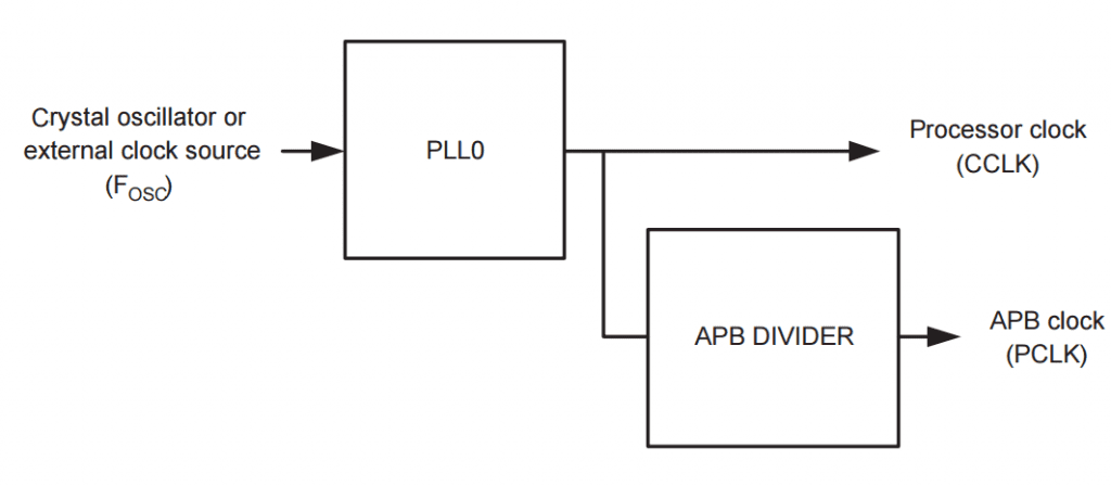
The following image shows the block diagram of PLL, CCLK and PCLK.
The value in the VPBDIV register determines the PCLK value. The following table shows the possible values of VPBDIV and the corresponding PCLK values.
| VPBDIV = 0x00 | PCLK is ¼ of CCLK |
| VPBDIV = 0x01 | PCLK is equal to CCLK |
| VPBDIV = 0x02 | PCLK is ½ of CCLK |
| VPBDIV = 0x03 | Reserved. No effect. |
We have seen all the registers, settings and necessary calculations in order to configure PLL0. For more information about this, we can look up to the data sheet and user manual of LPC214x series of MCUs.
Now, we’ll see an example program for configuring the PLL0 so that the CPU Clock (CCLK) and the Peripheral Clock (PCLK) must run at 60 MHz with an external crystal oscillator operating at 12 MHz.
Note: 12 MHz is the most common value for crystal oscillator in many microcontroller development boards. If the development you are using has a different crystal oscillator (for some strange reason), then we need to consider the values of ‘M’ and ‘P’.
#define PLOCK 0x00000400
int main(void)
{
/* PPLE = 1 and PPLC = 0 so PLL0 will be enabled but not connected. */
PLL0CON = 0x01;
/* PLL0CFG is set as per the table mentioned above. */
PLL0CFG = 0x24;
/* Feed Sequence for locking PLL0 to desired frequency */
PLL0FEED = 0xAA;
PLL0FEED = 0x55;
/* Check whether the PLL0 has locked on to the desired frequency by reading the lock bit
in the PPL0STAT register */
while( !( PLL0STAT & PLOCK ));
/* Now enable(again) and connect the PLL0 */
PLL0CON = 0x03;
/* Feed Sequence for connecting the PLL0 as system clock */
PLL0FEED = 0xAA;
PLL0FEED = 0x55;
/* Now the System Clock is running @ 60 MHz! Next step is to set the Peripheral Clock at same frequency as System Clock */
VPBDIV = 0x01;
while(1);
}

5 Responses
Very precise explanation! Thanks a lot
Thanks a lot for such a wonderful explanation
This is exactly what I’m looking for…………..very deep explanation and it makes the whole topic too easy to understand………..thank you so much
very very clear explanation….thank you so much….
how can we get 40mhz frequency