In this tutorial, we will learn about Active Band Pass Filter, its frequency response, types, examples and many more. In a previous tutorial, we have seen about Band Pass filters but the design approach in that tutorial was based on passive components.
Band Pass Filter, like any other filter, can be designed around active components like Transistors and Op-amps. If you want more information on Passive Band Pass Filers, read “Passive Band Pass RC Filter“.
Introduction
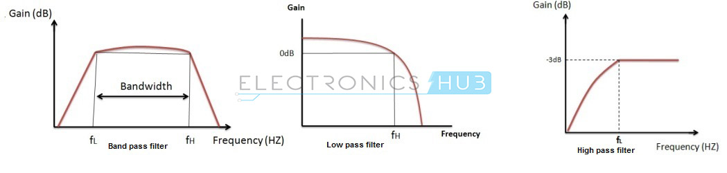
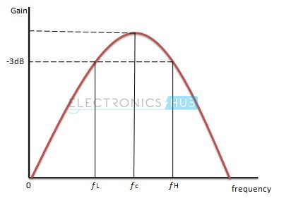
A Band Pass Filter is a circuit which allows only particular band of frequencies to pass through it. This Pass band is mainly between the cut-off frequencies and they are fL and fH, where fL is the lower cut-off frequency and fH is higher cut-off frequency.
The centre frequency is denoted by ‘fC’ and it is also called as resonant frequency or peak frequency.
The fL value must always be less than the value of fH. The pass band of the filter is nothing but the bandwidth. The gain of the filter is maximum at resonant or centre frequency and this is referred as total pass band gain. This pass band gain is denoted by ‘Amax’.
For low pass filter this pass band starts from 0 Hz and continues until it reaches the resonant frequency value at -3 dB down from a maximum pass band gain.
Where as in the case of high pass filter this pass band begins from the -3 dB resonant frequency and ends at the value of the maximum loop gain for active filter. Combination of low pass and high pass responses gives us band pass response as shown below:
Active Band Pass Filter
Depending on the quality factor the band pass filter is classified into Wide band pass filter and Narrow band pass filter. The quality factor is also referred as ‘figure of merit’. By cascading High Pass Filter and Low Pass Filter with an amplifying component we obtain band pass filter.
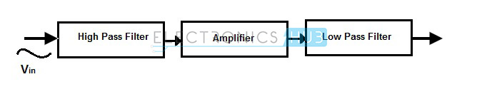
The amplifier circuit between these high pass and low pass filter will provide isolation and gives over all voltage gain of the circuit. The values of the cut-off frequencies of both the filters must be maintained with minimum difference.
If this difference is very small, there may be a possibility of interacting of high pass and low pass stages. Thus, in order to have proper levels of these cut-off frequencies an amplifying circuit is necessary.
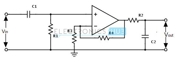
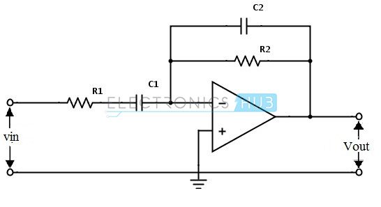
The circuit diagram for active band pass filter is shown below:
Wide Band Pass Filter
If the value of quality factor is less than ten, then the pass band is wide, which gives us the larger bandwidth. This band pass filter is called Wide Band Pass Filter.
In this filter the high cut-off frequency must be greater than the lower cut-off frequency. It uses two amplifying elements (Op-amps) in design.
First the signal will pass through the high pass filter, the output signal of this high pass filter will tends to infinity and thus the signal which tends to infinity is given to the low pass filter at the end.
This low pass filter will low pass the high frequency signal.
When the High Pass Filter is cascaded with Low pass filter the simple Band Pass Filter is obtained. In order to realise this filter the order of the low pass and high pass circuits must be same.
By cascading one first order low pass and high pass gives us the second order band pass filter and by cascading two first order low pass filters with two high pass filters forms a fourth order band pass filter.
Due to this cascading the circuit produces a low value quality factor. The capacitor in the first order high pass filter will block any DC biasing from the input signal.
The gain rolls off at both the stop bands is ± 20 dB /decade in the case of second order filter (High + Low). The high Pass and low pass filters must be in first order only.
Similarly, when the high pass and low pass filters are at second order, then the gain roll off at both the stop bands is ± 40dB/Decade.
The voltage gain expression for band pass filter is given as:
| Vout / Vin | = [Amax * (f/fL)] / √{[1+(f/fL)²][1+(f/fH)²]}
It is obtained by the individual gains of both high pass and low pass filters, the individual gains of both high pass and low pass filter are given below.
Voltage Gain for High Pass filter:
| Vout / Vin | = [Amax1 * (f/fL)] / √[1+(f/fL)²]
Voltage Gain for Low pass filter:
| Vout / Vin | = Amax2 / √[1+(f/fH)²]
Amax = Amax1 * Amax2
Where Amax1 is the gain of the high pass stage and Amax2 is the gain of the low pass stage.
The response of the wide band filter is shown below.
Narrow Band Pass Filter
If the value of quality factor is greater than ten then the pass band is narrow and bandwidth of the pass band is also less. This band pass filter is called as Narrow Band Pass Filter.
It uses only one active component (op-amp) rather than two and this op-amp is in inverting configuration. In this filter the gain of the op-amp is maximum at centre frequency fc.
Narrow Band Pass Filter Circuit
The input is applied to the inverting input terminal. This shows that the Op-amp is in inverting configuration. This filter circuit produces narrow band pass filter response.
The voltage gain of the above filter circuit is AV = – R2 / R1
The cut-off frequencies of the filter circuit are
fC1 = 1 / (2πR1C1) and fC2 = 1 / (2πR2C2)
Multi Feedback Active Band Pass Filter
This filter circuit produces a tuned circuit based on the negative feedback of the filter. The important advantage of this multiple feedback is that without any change in the maximum gain at the centre frequency we can change the value of the cut-off frequency. This change in the cut-off frequency can be done by the resistance ‘R3’.
By considering the below active filter circuit, let us consider the changed resistor value as R3′and the changed cut-off frequency value as fc′, then we can equate for the new resistor value as follows:
R3′ = R3(fc /fc′)²
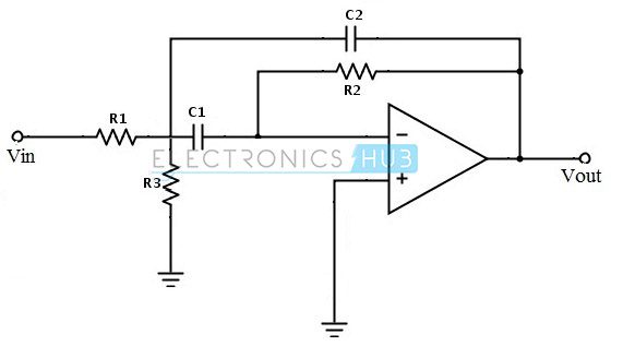
It consists of two feedback paths, because of this multiple feedback paths it is also referred as ‘Multiple feedback band pass circuit’. This circuit produce an infinity gain multiple feedback band pass filter. Due to this circuit the quality factor value increases maximum up to 20.
fc = 1/√(R1R2C1C2)
Q = fc/Bandwidth = (½){√[R2/R1]}
Amax = -R2/2R1
R1 = Q/{2πfcCAmax}
R2 = Q/πfcC
R3 = Q/{2πfcC(2Q² – Amax)}
The gain at the centre frequency ‘Amax’ must be less than 2Q². That is,
Amax < 2Q²
Where,
fc = cut off frequency in Hz
C = Capacitance, (C1 = C2 = C)
Q = Quality factor
Amax = Maximum gain
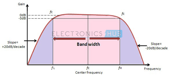
The Frequency Response of Active Band Filter
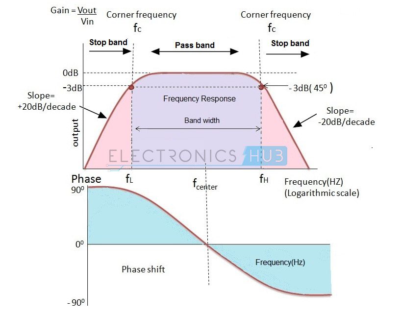
It has two centre frequencies, one is of high pass filter and the other is of low pass filter. The centre frequency of the high pass filter must be lower than the centre frequency of the low pass filter.
The centre frequency of band pass filter is the geometric mean of lower and upper cut-off frequencies fr2 = fH * fL.
The gain of the filter is 20 log (Vout/Vin) dB/Decade. The amplitude response is similar to the responses of the low pass and high pass filter. Depending upon the cascading filter order the response curve depends.
The normalized mid frequency is given as fr = 1. Let us consider two cut-off frequencies as 300 Hz and 900Hz, then, the bandwidth of the filter is 300 Hz -900 Hz = 600 Hz.
The Quality Factor
The quality factor depends on the bandwidth of the pass band. Quality factor is inversely proportional to the Bandwidth. That means if band width increases the quality factor decrease and if band width decreases the quality factor increases.
Q = fc/Bandwidth
For wide band pass filter the quality factor is low because the pass band width is high. For the narrow band pass filter the quality factor is high. Selectivity and un-selectivity depends on the width of the pass band.
This quality factor is also relates to the damping factor (). If damping co-efficient value is more the flatness of the output response also more. This is equated as follows:
ε = 2/Q
For different quality factor values the normalized gain response of a second order band pass filter is given as:
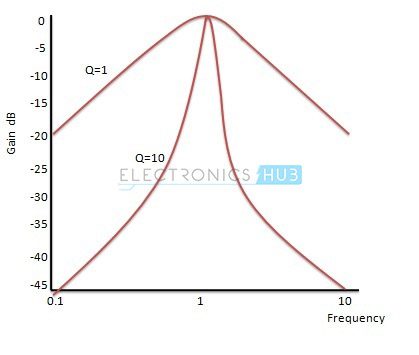
By this graph, it is clear that the selectivity is more for higher quality factor.
Active Band Pass Filter Example
Let us consider the infinity gain multiple feedback active filter circuit for which the resonating frequency is 1.5 kHz, maximum Voltage gain is 15 and quality factor is 7. Then component values are calculated as follows:
For Resistors
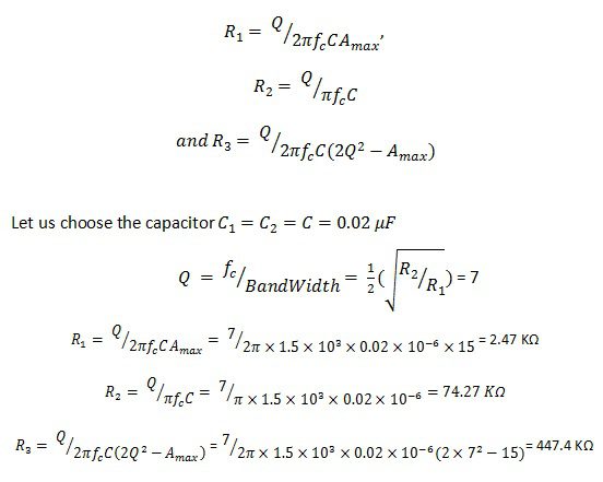
We consider that the changed resistor value as R3´ and the changed cut-off frequency value fc´=2 KHz then we can equate for the new resistor value as follows:
R3´ = R3 (fc/fc´)2 = 447.4(1.5/2)2 = 251.66 Ω
Therefore simply by taking the required frequency we can calculate the new resistor value.

6 Responses
So helpful for electronic s students
i want to ask about the values of resistors and capacitors if u please in active band pass filter circuit !!
In Multi Feedback Active Band Pass Filter, how to find voltage output if voltage input is 3Vpp and the frequency is 50Hz, 100Hz, 500Hz, and 1KHz.
R1 = 68K
R2 = 180k
R3 = 2.7k
C=C1=C2= 0.01uF
Can we cscade a low pass and high pass filter in wide band pass filter?
I had a question about the calculations. if Q=7 then 7=1/2(sqrt(r2/r1)) but for the values we get for r2 and r1 this doesn’t seem to work? Am I missing something I get like 2.74 which obviously isn’t q. Can you elaborate on what I am missing?
Explain a single active bandpass filter circuit act as wideband as well as narrow bandpass filter, give the common circuit and calculations