This circuit helps you to manage your appliances in your home devoid of getting off from your bed. All you need is to just clap or you can puff in front of the microphone and after that, the device attached to the microphone becomes “ON” or “OFF”.
The plus points of this circuit are as follow:
- At the same time, you can either “ON” or “OFF” up to three devices.
- To “ON” or “OFF” the device, it is not necessary for you to shift from your place.
- It will give you visual indication of the appliances also like it is “ON” or “OFF”.
Related Post: Clap Switch Circuit for Devices
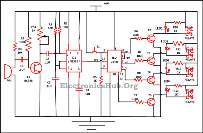
9 Way Clap Switch Circuit Diagram:
- IC
- NE555 – 1
- 7490 – 1
- Resistor
- R1, R2 (10K) – 2
- R3, R4 (100K) – 2
- R6, R7, R8, R9 (100E) – 4
- R10, R11, R12, R13, R5 (1K) – 5
- VR1 (1K) – 1
- C1,C2,C3,C4(.1uf) – 4
- T1 (BC548) – 1
- T2,T3,T4,T5(BC547) – 4
- LED – 3
- MIC – 1
- RELAY – 4
- Switch – 1
9 Way Clap Switch Circuit Description:
This circuit is mainly built in the region of the two IC’s along with a few other components –
1. NE555 Timer – This IC is basically configured in the monostable state. In this mode, the 555 works like a “one-shot” pulse producer. Applications comprise timers, lost pulse recognition, bounce free switches, contact switches, frequency separator, capacitance measurement, pulse-width modulation (PWM) and lots of more.
IC 555 timer is a one of the far and wide used IC in the field of electronics and is employed in different varieties of electronic circuits for its properties like robustness and stability. It is used to produce square-wave having duty cycle with a range from 50% to 100%, Oscillator can also offer time delay in circuits. The 555 timer got its forename from the three 5k ohm resistor coupled in a voltage-divider pattern.
The circuit used to make a 555 timer in monostable is:
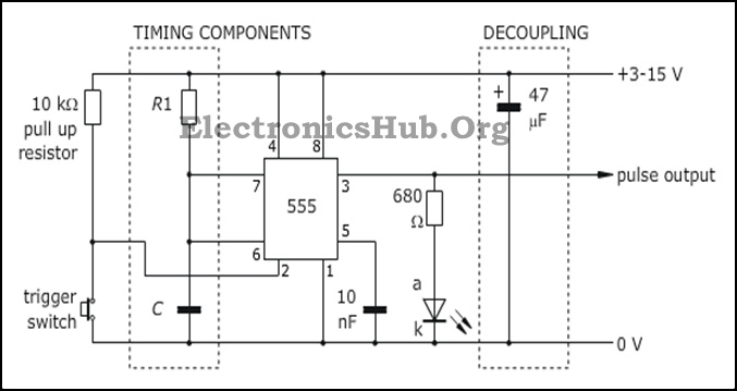
As you can observe, the trigger input is detained HIGH by the 10 kΩ drag up resistor moreover is pulsed LOW at the time the trigger switch is pushed. The circuit is triggered by a declining edge, that is, by a rapid move from HIGH to LOW.
The trigger pulse, created by pressing the button, has to be of less period than the proposed output pulse.
The period, t, of the output pulse can be calculated from the design equation:
T=1. 1 (R*C)
2. IC 7490 – This IC is basically a decade as well as a binary counter. This IC holds four master slave flip flop along with divided by two as well as divided by five counter. It can also be employed as divided by 9 counter by linking Q0 by the clock input pin1 (CP1) and in addition to it giving clock pulse to CP0 which is on pin 14. This IC can also be worked like a divided by 6 counter by just linking Q0 along with CP0 and providing input pulse at CP1.
9 different ways of combinations are being provided by the IC 7490 for “ON “ and “OFF” of the four totally different appliances in 9 claps. In the same way, 7492 IC is as well available in the market which will give you 11 fully different groups of output for the purpose of controlling the four numbers of appliances. And one more type of IC that is 7493 is available in the market which offers 15 different varieties to hold the four appliances.
When you clap or puff on face of the microphone, microphone transferred the sound of clapping into the electrical energy. Now, the transistor which works as a preamplifier enlarges these week signals. With the help of variable resistor VR1, the sensitivity of the signal can be enhanced. Now the output from the transistor T1 is supplied to the monostable circuit which connects to NE555 IC.
At the time you clapped in front of the microphone, pin 3 output of IC1 moves to high state and this is given to the pin 14 clock input of IC2. Now the output of IC2 is given to the transistor T2-T4 with the help of 100 ohm resistor to drive the related relay attached to it. To indicate the states of the different appliances, different colors of LED is also connected with the circuit. Glowing of the LED indicates that the appliance is “ON” while if LED will not glow it indicates that the device is”OFF”. The stages of the output for IC7490 (Q0-Q3) for the different number of claps is being displayed in the table below.
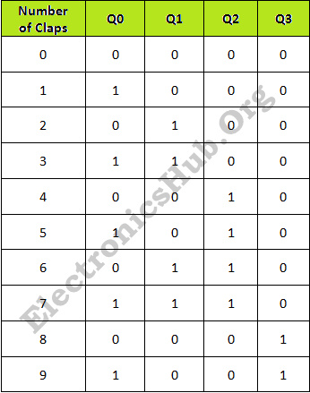
In the above table, logic 1 shows that the corresponding transistor carries out to energize the equivalent relay and the device linked with it activated. While the logic 0 in the above table shows that the device is inactive state.

4 Responses
Can you please specify which RELAY we have to use?
Which Relay is use kindly tell me?
Dear
According to the voltage of power supply which is 6 volt, you can use most 6 volt relays. The only minor thing is the current of the coil of relay should not increase the permissible current of the transistors 2-5. Whatever transistors you use there check its permissible current in Data Sheet. In this case we have used BC547: transistor
The BC548 is a general-purpose NPN bipolar junction transistor
Pinout and specifications
Lead 1 (left in diagram) is the collector
Lead 2 is the base
Lead 3 is the emitter (right in diagram)
Do not use it with more than 25 voltage and more than 90 milliamps.
So your relay coil can be (in this case) 6 volt with 90 milliamps. Which is quite fine!
S.J. Sayyedi
Sir which type of relay is used please